Flip LED chip structure and manufacturing method thereof
A technology of LED chips and manufacturing methods, which is applied in the direction of electrical components, circuits, semiconductor devices, etc., can solve the problems of the overall volume of the lens, the height is huge, the level of the maximum illuminance is restricted, and the method of substrate processing is scarce, so as to improve the light extraction. Efficiency, avoiding light loss, and reducing the effect of total reflection loss
- Summary
- Abstract
- Description
- Claims
- Application Information
AI Technical Summary
Problems solved by technology
Method used
Image
Examples
Embodiment 1
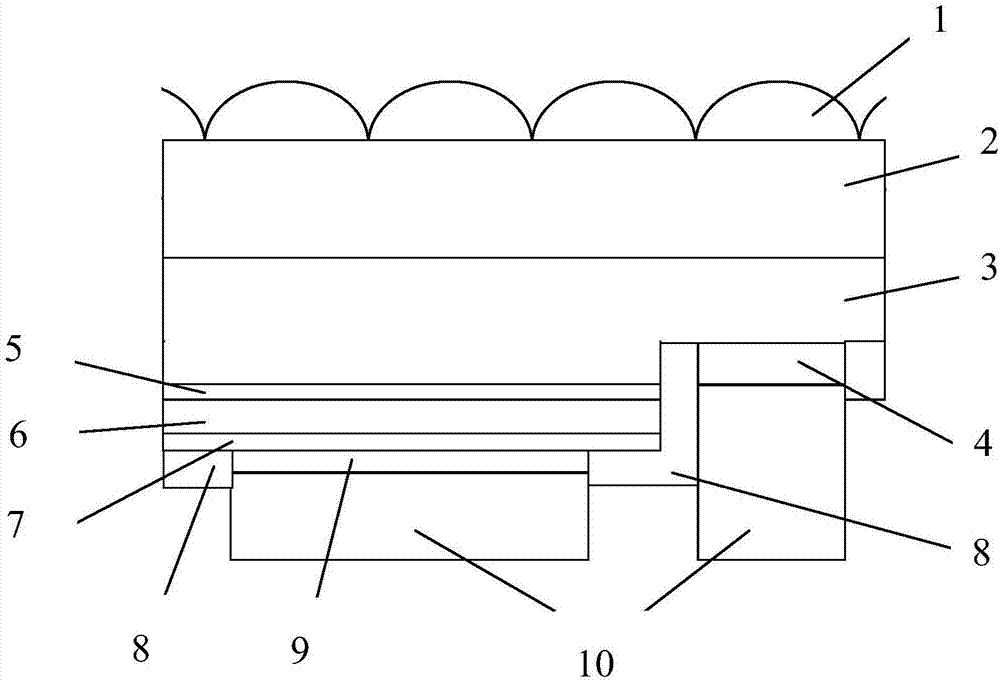
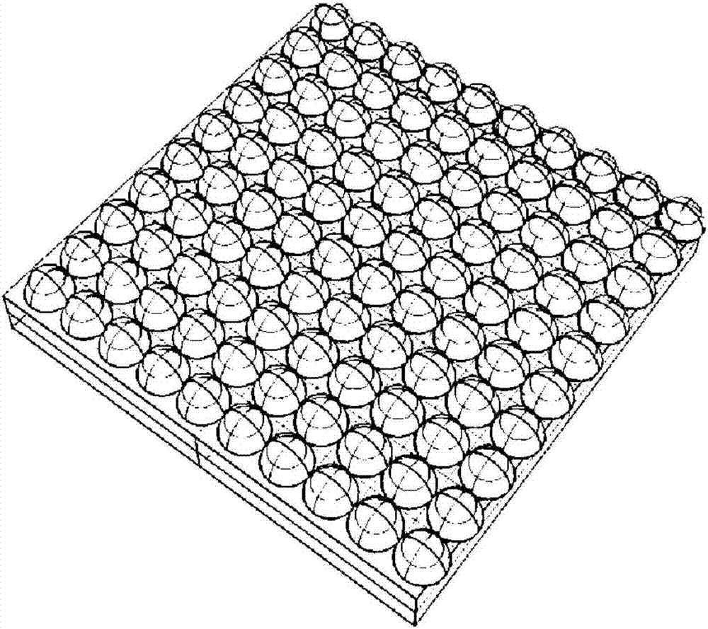
[0049] Embodiment 1 of the present invention: as figure 2 As shown, the two-dimensional periodic array lens in the three-dimensional graphic structure 1 is composed of multiple groups of hemispherical convex units, forming a three-dimensional diagram of two-dimensionally arranged hemispherical collimating lenses. The substrate processing pattern of the light-emitting surface of the chip is a two-dimensional array of hemispheres, which has a collimating effect on light-emitting.
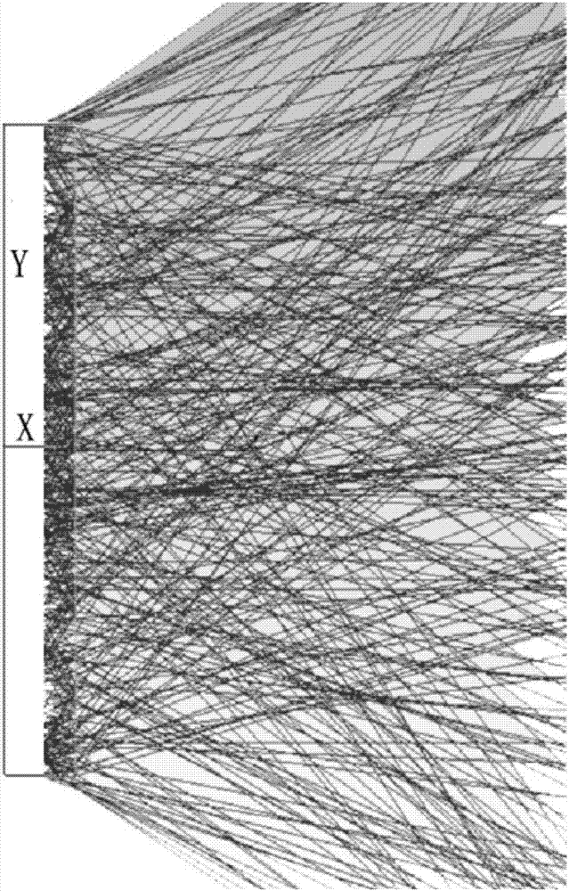
[0050] Such as image 3 As shown, the ordinary flip-chip LED chip simulates the light effect diagram, such as Figure 5 As shown, the simulated light effect diagram after adding a two-dimensional array of hemispheres on the sapphire substrate 2, after comparing the simulated light effect diagrams of the two, it is found that changing the state of the original mirror surface of the flip-chip LED chip and adding a hemispherical array Finally, it can change the light intensity distribution, reduce or ...
Embodiment 2
[0061] Embodiment 2 of the present invention: as Figure 5 As shown, the one-dimensional periodic array lens in the three-dimensional graphic structure 1 has an array pattern of a one-dimensional array of semi-cylindrical strips, and multiple groups of semi-cylindrical strips form a three-dimensional diagram of one-dimensionally arranged collimating lenses. The pattern can achieve light collimation in the periodic direction, but does not produce light collimation in the cylindrical direction, and can reduce or avoid the loss of light output by the secondary optical system.
[0062] The chip manufacturing steps of the present embodiment are as follows, wherein the mask material is photoresist:
[0063] Step 1: using MOCVD (metal organic compound chemical vapor deposition) equipment to deposit an LED structure semiconductor material layer on the sapphire substrate 2, including an N-type semiconductor material 3, a light-emitting layer 5, and a P-type semiconductor material 6;
...
PUM
| Property | Measurement | Unit |
|---|---|---|
| Thickness | aaaaa | aaaaa |
Abstract
Description
Claims
Application Information


