LED (Light Emitting Diode) chip photoetching developing method

A technology of LED chip and development method, applied in optics, photography, optomechanical equipment, etc., can solve the problem of high production cost of photolithography development process, achieve low cost, fast development speed, and reduce production cost

Inactive Publication Date: 2017-09-05
XIANGNENG HUALEI OPTOELECTRONICS
View PDF3 Cites 3 Cited by
  • Summary
  • Abstract
  • Description
  • Claims
  • Application Information

AI Technical Summary

Problems solved by technology

[0006] In view of this, the present invention provides a method for photolithography and development of LED chips, which solves the problem of high production cost of LED chip photolithography and development in the prior art

Method used


Image

  • LED (Light Emitting Diode) chip photoetching developing method
  • LED (Light Emitting Diode) chip photoetching developing method
  • LED (Light Emitting Diode) chip photoetching developing method

Examples


Embodiment 1

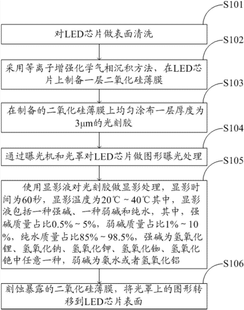
[0032] refer to figure 1 , figure 2 , image 3 with Figure 4 , the embodiment of the present invention provides a LED chip photolithographic development method, comprising the following steps:

[0033] Step S101: cleaning the surface of the LED chip;

[0034] Step S102: preparing a layer of silicon dioxide film on the LED chip by using the plasma enhanced chemical vapor deposition method;

[0035] Step S103: uniformly coating a layer of photoresist with a thickness of 3 μm on the prepared silicon dioxide film;

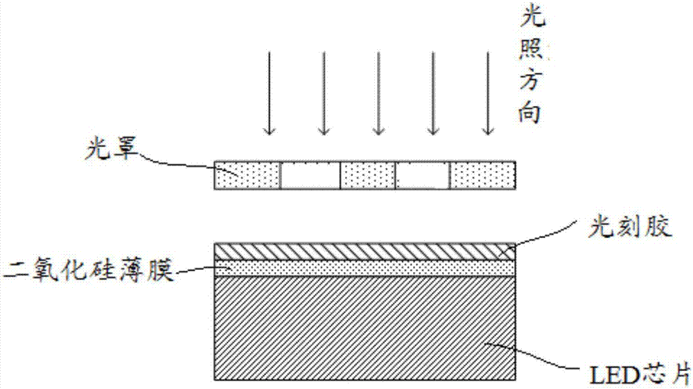
[0036] Step S104: Perform graphic exposure processing on the LED chip through the exposure machine and the mask, and the schematic diagram of the exposure processing on the LED chip is as follows: figure 2 shown;

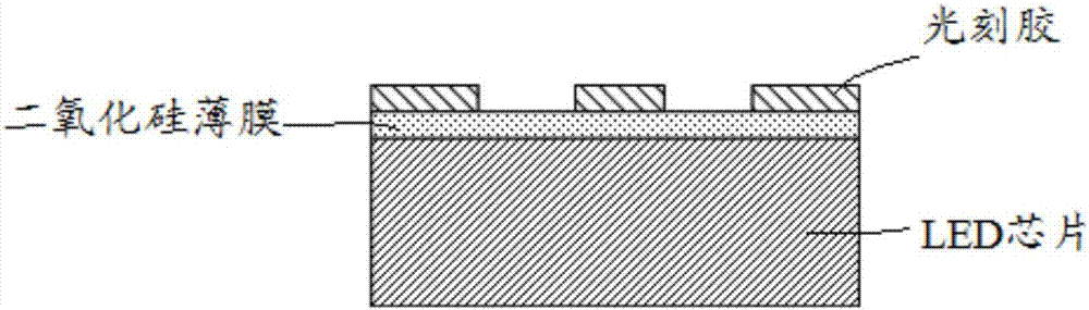
[0037] Step S105: Use a developer to develop the photoresist. The developing time is 60 seconds, and the developing temperature is 20°C-40°C. The schematic diagram of the structure of the LED chip after the developing process is as follows: image ...

Embodiment 2

[0043] This embodiment provides a preferred LED chip photolithographic development method. In the LED chip photolithographic development method provided by this embodiment, the same steps as those in the above-mentioned embodiment 1 will not be repeated here. The main difference is that this embodiment In 2, when using the developing solution to develop the photoresist, the preparation method of the developing solution is as follows:

[0044] The raw materials for developer preparation are potassium hydroxide with a mass fraction of 38% to 40%, ammonia water and pure water with a mass fraction of 25% to 28%;

[0045] Under the temperature condition of 18°C ​​to 25°C, first weigh a certain amount of potassium hydroxide, then add a certain amount of pure water, stir evenly, and finally add a certain amount of ammonia water, stir evenly, and finally obtain potassium hydroxide with a mass ratio of 2 %, the ammonia water mass accounts for 5%, and the pure water mass accounts for 93...

Embodiment 3

[0048] This embodiment provides a method for photolithography and development of LED chips, including the following steps:

[0049] Step S201: cleaning the surface of the LED chip to remove pollutants, particles, organic matter, etc. on the surface of the LED chip;

[0050] Step S202: preparing a layer of silicon dioxide film on the LED chip by using the plasma enhanced chemical vapor deposition method;

[0051] Step S203: Evenly coat a layer of photoresist with a thickness of 3 μm on the prepared silicon dioxide film, specifically, add photoresist on the LED chip, and rotate the LED chip at a speed of 1000-2000 rpm for uniform coating. Adhesive, LED chip speed and photoresist addition amount and viscosity match to ensure uniform coating of photoresist;

[0052] Step S204: Place the LED chips evenly coated with photoresist in an oven, and bake them at 95°C for 2 minutes, pre-bake the LED chips evenly coated with photoresist, and remove the particles in the photoresist. Solve...


PUM

PropertyMeasurementUnit
quality scoreaaaaaaaaaa

Abstract

The invention discloses an LED (Light Emitting Diode) chip photoetching developing method which comprises the following steps: cleaning the surface of an LED chip; by using a plasma enhanced chemical vapor deposition method, preparing a layer of a silicon dioxide membrane on the LED chip; uniformly coating the prepared silicon dioxide membrane with a layer of a photoresist of 3mu m in thickness; performing graphic exposure treatment on the LED chip through an exposure machine and a light cover; performing development treatment on the photoresist by using a developing liquid, wherein the developing time is 60 seconds, the developing temperature is 20-40 DEG C, the developing liquid comprises strong base, weak base and pure water, the strong base accounts for 0.5-5% by mass, the weak base accounts for 1-10% by mass, the pure water accounts for 85-98.5% by mass, the strong base is any one of lithium hydroxide, sodium hydroxide, potassium hydroxide, rubidium hydroxide and cesium hydroxide, and the weak base is ammonia water or aluminum hydroxide; and etching the exposed silicon dioxide membrane, and transferring patterns on the light cover to the surface of the LED chip.

Description

technical field [0001] The present invention relates to the technical field of semiconductors, and more specifically, to a photolithography and developing method for LED chips. Background technique [0002] A light emitting diode (Light Emitting Diode, LED) is a semiconductor electronic component that can convert electrical energy into light energy, and is widely used in fields such as displays, lighting, warning lights, and colored light decorations. [0003] Photolithography development is one of the important process steps in LED manufacturing. This process removes a specific part of the film on the surface of the LED chip through a series of process steps, and then forms a film with a characteristic graphic structure on the surface of the LED chip. [0004] A photoresist developer is used in the photolithography development process step, and the developer is generally an alkaline aqueous solution. The most common positive resist developing solution is Tetramethylammoniu...

Claims


Application Information

Patent Timeline
Patent Type & Authority Applications(China)
IPC IPC(8): G03F7/30G03F7/32G03F7/16G03F7/40
CPCG03F7/162G03F7/30G03F7/322G03F7/40
Inventor 袁章洁张力
Owner XIANGNENG HUALEI OPTOELECTRONICS
Why Eureka
Try Eureka