Surface processing technology for improving GaN HEMT passivation effect and reducing current collapse

A surface treatment and technology technology, applied in the field of microelectronics, can solve the problems of incomplete removal of gallium nitride surface, reduce surface passivation, aggravate current collapse, etc., and achieve the effect of stable thickness, easy control and wide use

Inactive Publication Date: 2017-09-12
PEKING UNIV
View PDF4 Cites 4 Cited by
  • Summary
  • Abstract
  • Description
  • Claims
  • Application Information

AI Technical Summary

Problems solved by technology

At present, the commonly used methods in the industry include surface treatment based on nitrogen, ammonia, and oxygen plasma, but the plasma will cause damage on the surface of GaN, which will further aggravate the current collapse; and the above-mentioned surface cann

Method used


Image

  • Surface processing technology for improving GaN HEMT passivation effect and reducing current collapse
  • Surface processing technology for improving GaN HEMT passivation effect and reducing current collapse
  • Surface processing technology for improving GaN HEMT passivation effect and reducing current collapse

Examples


Embodiment Construction

[0031] Hereinafter, the present invention will be more fully described with reference to the accompanying drawings, so that the technical means, creative features, work flow, and usage methods of the present invention can be easily understood. The described embodiment is only one form of implementation of the invention, ie the invention should not be construed as limited to the embodiments set forth herein. Based on the embodiment, the scope of the present invention is fully conveyed to those skilled in the art.

[0032] Hereinafter, exemplary embodiments of the present invention will be described in more detail with reference to the accompanying drawings. Its preparation method comprises the following specific steps:

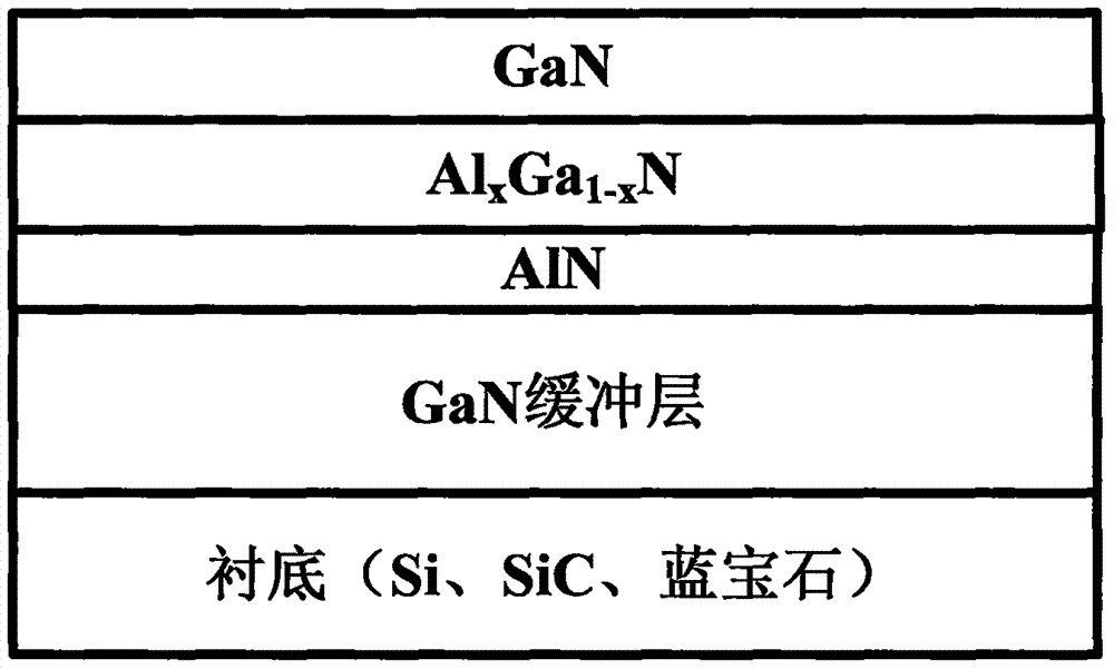
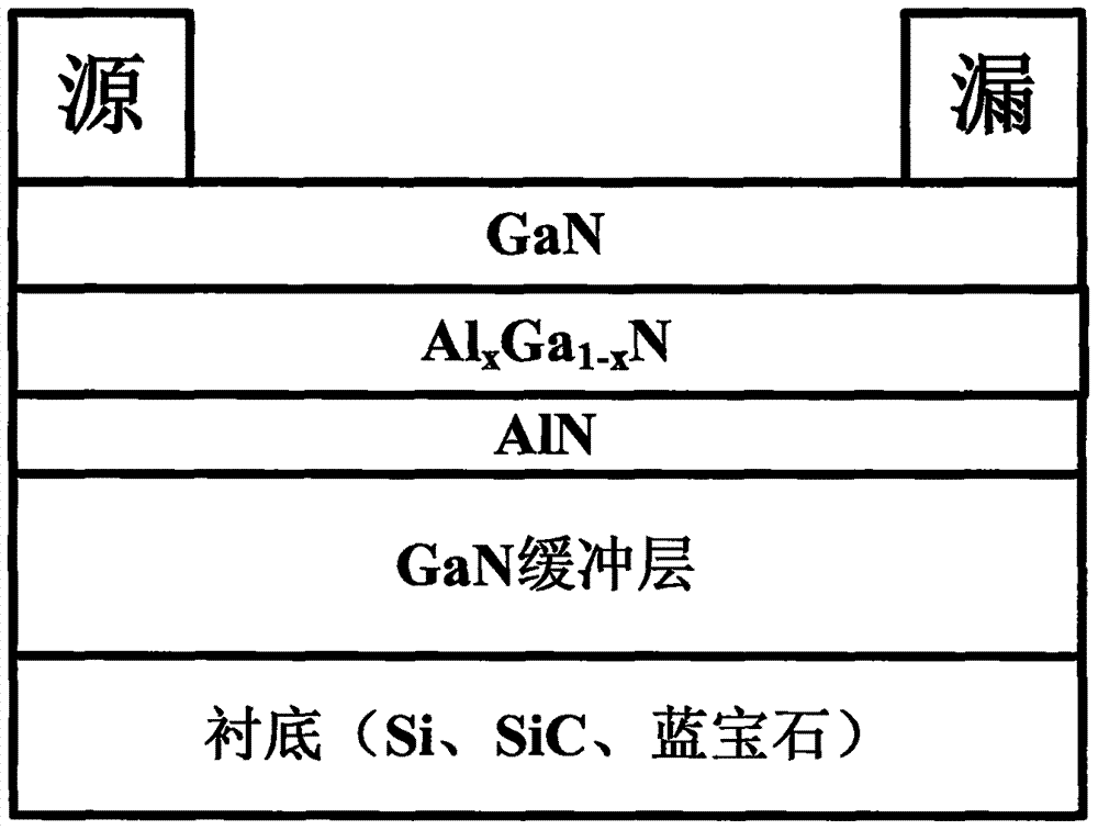
[0033] (1) if figure 1 As shown, on a Si substrate (the substrate can also be SiC or sapphire), a GaN channel layer is first grown by MOCVD, an AlN insertion layer is grown on it, and 24nm AlGaN is grown, and finally GaN is grown Surface capping layer.

[...


PUM

PropertyMeasurementUnit
Thicknessaaaaaaaaaa
Thicknessaaaaaaaaaa
Thicknessaaaaaaaaaa

Abstract

The present invention discloses a surface processing technology and a method for improving the surface passivation effect of the gallium nitride-based electronic device and reducing the current collapse. The method is mainly applied to the preparation of the gallium nitride-based electronic device, before the conventional passivation layer deposition, ozone, oxygen plasma and other strong oxidants are used on the surface of gallium nitride for oxidation, then hydrochloric acid is used to remove a thin layer of oxide, and the process is repeated for a number of cycles before the surface passivation to completely remove surface defects, so as to get a relatively perfect surface, thereby improving the surface passivation effect, reducing the current collapse caused by the surface trapping effect.

Description

technical field [0001] The invention belongs to the technical field of microelectronics and relates to the preparation of gallium nitride-based electronic devices Background technique [0002] GaN materials have attracted much attention due to their superior properties such as large band gap, high saturation electron drift velocity, strong critical breakdown electric field, and high thermal conductivity. Compared with other III-V semiconductor materials, the GaN-based heterojunction can generate a very high concentration of two-dimensional electron gas through a strong spontaneous polarization effect when it is not doped, making it the third-generation semiconductor material. first choice. The superior performance of GaN material makes it have broad application prospects in the fields of radio frequency microwave and power electronics. [0003] GaN-based electronic devices are mainly based on AlGaN / GaN heterojunction structures. As mentioned above, in the conventional AlG...

Claims


Application Information

Patent Timeline
IPC IPC(8): H01L21/02H01L21/335
CPCH01L29/66431H01L21/02271
Inventor 王茂俊林书勋陶明郝一龙
Owner PEKING UNIV
Why Eureka
Try Eureka