DMD-based dual-mode optical super-resolution microscopic imaging device and method
A microscopic imaging and optical imaging system technology, which is applied in the field of dual-mode optical super-resolution microscopic imaging devices, can solve the problems of complex optical path system and cost reduction, and achieve cost reduction, lower threshold, high stability and ease of use Effect
- Summary
- Abstract
- Description
- Claims
- Application Information
AI Technical Summary
Problems solved by technology
Method used
Image
Examples
Embodiment 1
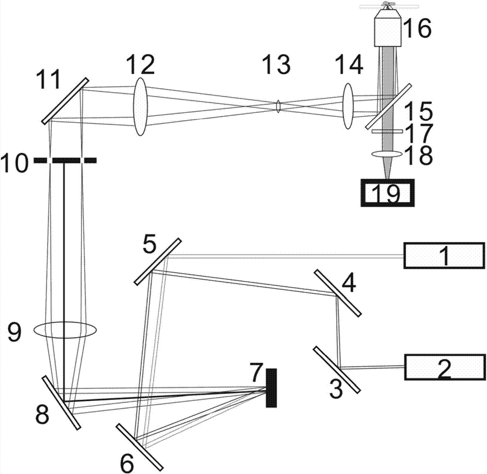
[0041] In this embodiment, the dual-mode optical super-resolution microscopic imaging device based on DMD is as follows: figure 1 As shown, among them, 1 is a semiconductor laser with a wavelength of 532nm, and 2 is a semiconductor laser with a wavelength of 405nm. Two kinds of lasers with different wavelengths can be selected according to actual imaging needs. 3, 4, 5, 6, 8, and 11 are plane mirrors with adjustable angles, 7 is a DMD chip, 9, 12, and 14 are lenses, 10 is a mask for diffraction spot gating, and 13 is an aperture stop , 15 is a 545nm long-pass dichroic mirror, 16 is an objective lens, 17 is a fluorescence filter, 18 is an imaging lens, and 19 is a sCMOS camera.
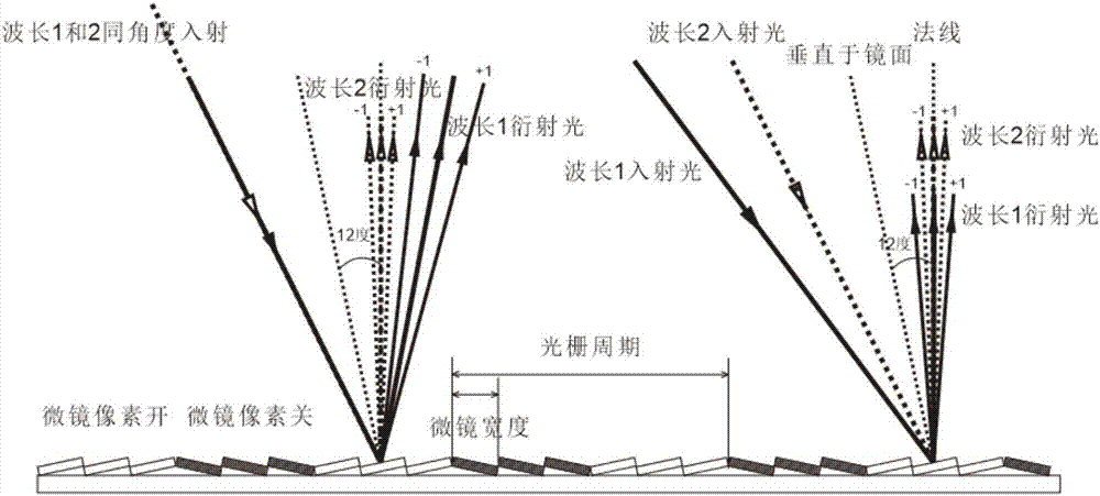
[0042] The super-resolution microscopic imaging device described in this embodiment is divided into the following parts according to the functions realized, which are two lasers, a laser modulation module, a microscope optical imaging system and an object stage, and the laser modulation module includes...
Embodiment 2
[0049] This embodiment is based on Figure 8 The shown device realizes single-molecule localization imaging SMLM, and its steps are:
[0050] In the same optical path system as in Embodiment 1, the single-hole mask shown in Figure 5 (b) is inserted at the position of the gate mask 10, and a single diffraction spot (such as Figure 8 shown). Control the DMD chip to switch between black and white stripes of two different spatial frequencies K1 and K2, so that the laser spots with wavelengths of 405nm and 532nm alternately pass through the small holes of the mask to obtain alternating light pulses (as shown in Figure 9 (a, b)). Use corresponding switchable fluorescent dyes, such as Alexa-fluo 532, to label cell samples. The dye molecules are randomly converted into active states under 405nm laser irradiation, and excited to emit fluorescence under 532nm laser irradiation, which is detected and recorded by a high-sensitivity camera down.
[0051] The DMD pattern controller cont...
PUM
| Property | Measurement | Unit |
|---|---|---|
| wavelength | aaaaa | aaaaa |
| wavelength | aaaaa | aaaaa |
Abstract
Description
Claims
Application Information


