Ferroelectric thin-film transistor and preparation method thereof

A ferroelectric thin film and transistor technology, applied in the direction of transistor, semiconductor/solid-state device manufacturing, circuit, etc., can solve the problems of increasing process difficulty, increasing chip manufacturing cost, incompatibility, etc., and achieves the improvement of CMOS logic circuit application, less leakage and Excellent breakdown and thermal stability

Active Publication Date: 2017-09-15
XIANGTAN UNIV
View PDF1 Cites 19 Cited by
  • Summary
  • Abstract
  • Description
  • Claims
  • Application Information

AI Technical Summary

Problems solved by technology

However, the main problems of traditional ferroelectric memory are: (1) the storage density of FeRAM is low, and the current maximum capacity is 128Mbit; (2) it is not compatible with the silicon process platform; It contains highly chemically active heavy metal ions, and heavy metal ions are a fatal source of pollution that leads to the failure of integrated circuits; on the other hand, the preparation temperature of traditional ferroelectric thin films is high, which increases the difficulty of the process and increases the ferroelectric Cross Contamination of Thin Films and Silicon Integrated Circuits
This solution not only raises the development threshold of ferroelectric memory, but also increases the manufacturing cost of the chip
(3) The retention performance of FeFET did not meet the commercial requirements
Thin-film transistors are divided into bottom-gate and top-gate structures according to the position of the gate electrode. The bottom-gate structure is favored by people because of its simple manufacturing process. Compared with commercial ferroelectric memories, ferroelectric thin film transistors have a cell structure and The preparation process is simple, the interface characteristics between the ferroelectric thin film layer and the oxide semiconductor active layer are good, and it is easy to integrate in a large area. However, most of the current ferroelectric thin film transistors still use ferroelectric thin film materials such as traditional PZT and SBT, and generally require film thickness It shows good ferroelectric properties when it exceeds 60nm. In addition, the development of n-type semiconductor channel materials for thin film transistors has been greatly developed, but now it is difficult to prepare p-type devices. Some people doped ZnO with H, N and other elements. TFTs made of semiconductors show P-type characteristics, and there are also researches on the preparation of P-type TFTs by doping Li. In the past few years, there have been significant changes in the type of oxide as the active layer and the preparation process of TFT devices. Progress, the difficulty of preparing P-type transistors limits its application fields, such as low-power oxide-based integrated CMOS

Method used


Image

  • Ferroelectric thin-film transistor and preparation method thereof
  • Ferroelectric thin-film transistor and preparation method thereof

Examples


Embodiment 1

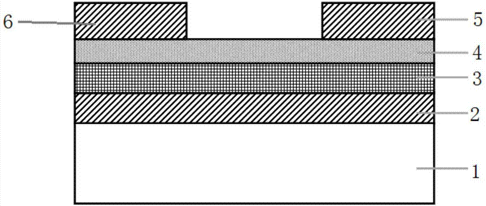
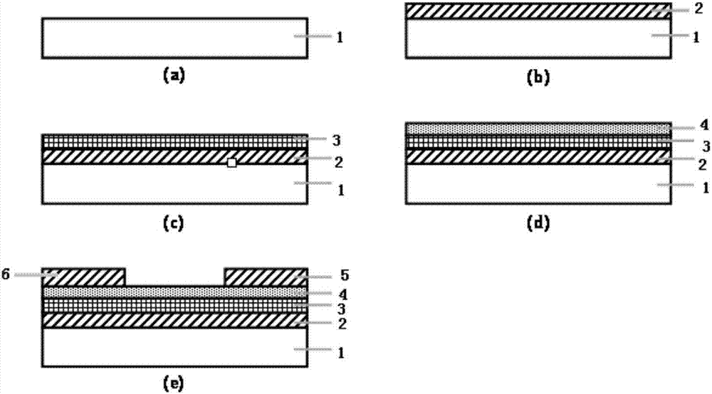
[0041] An embodiment of the ferroelectric thin film transistor of the present invention, a cross-sectional structure diagram of the ferroelectric thin film transistor described in this embodiment is shown in the attached figure 1 shown, including:

[0042] substrate1;

[0043] A bottom gate electrode 2 formed on the substrate 1;

[0044] A ferroelectric thin film layer 3 formed on the bottom gate electrode 2;

[0045] A channel layer 4 formed on the ferroelectric thin film layer 3;

[0046] a source electrode 5 formed on the channel layer 4;

[0047] as well as

[0048] A drain electrode 6 formed on the channel layer 4 and separated from the source electrode 5 .

[0049] The ferroelectric thin film layer 3 is composed of a hafnium oxide-based material, and the hafnium oxide-based material is Zr-doped HfO 2 Material; the thickness of the ferroelectric film layer 3 is 10nm; the substrate 1 is made of silicon material, and the thickness of the bottom gate electrode 2 is 120...

Embodiment 2

[0057] An embodiment of the ferroelectric thin film transistor of the present invention, a cross-sectional structure diagram of the ferroelectric thin film transistor described in this embodiment is shown in the attached figure 1 shown, including:

[0058] substrate1;

[0059] A bottom gate electrode 2 formed on the substrate 1;

[0060] A ferroelectric thin film layer 3 formed on the bottom gate electrode 2;

[0061] A channel layer 4 formed on the ferroelectric thin film layer 3;

[0062] a source electrode 5 formed on the channel layer 4;

[0063] as well as

[0064] A drain electrode 6 formed on the channel layer 4 and separated from the source electrode 5 .

[0065] The ferroelectric thin film layer 3 is composed of a hafnium oxide-based material, which is Si-doped HfO 2 Material; the thickness of the ferroelectric film layer 3 is 5nm; the substrate 1 is made of silicon material, and the thickness of the bottom gate electrode 2 is 100nm; the channel layer 4 is made ...

Embodiment 3

[0073] An embodiment of the ferroelectric thin film transistor of the present invention, a cross-sectional structure diagram of the ferroelectric thin film transistor described in this embodiment is shown in the attached figure 1 shown, including:

[0074] substrate1;

[0075] A bottom gate electrode 2 formed on the substrate 1;

[0076] A ferroelectric thin film layer 3 formed on the bottom gate electrode 2;

[0077] A channel layer 4 formed on the ferroelectric thin film layer 3;

[0078] a source electrode 5 formed on the channel layer 4;

[0079] as well as

[0080] A drain electrode 6 formed on the channel layer 4 and separated from the source electrode 5 .

[0081] The ferroelectric thin film layer 3 is composed of a hafnium oxide-based material, and the hafnium oxide-based material is Al-doped HfO 2 Material; the thickness of the ferroelectric thin film layer 3 is 20nm; the substrate 1 is made of silicon material, and the thickness of the bottom gate electrode 2 i...


PUM


Abstract

The invention discloses a ferroelectric thin-film transistor, which comprises a substrate; a bottom gate electrode formed on the substrate; a ferroelectric film layer formed on the bottom gate electrode; a channel layer formed on the ferroelectric film layer; a source electrode formed on the channel layer; and a drain electrode formed on the channel layer and separated from the source electrode. The invention also discloses a preparation method of the ferroelectric thin-film transistor. By introducing a hafnium-oxide-based material and SnO to the transistor to serve as a gate medium material and a channel material of the transistor respectively, the transistor is allowed to be compatible with existing silicon process in the preparation process, and can realize low power consumption; and the ferroelectric thin-film transistor can be widely applied to high-performance and low-power-consumption large-scale storage integrated circuits.

Description

technical field [0001] The invention relates to a transistor and a preparation method thereof, in particular to a ferroelectric thin film transistor and a preparation method thereof. Background technique [0002] The electronic information industry plays an extremely important role in expanding social employment, promoting economic growth, enhancing international competitiveness and maintaining national security. Memory, as the cornerstone of information computing and storage, shoulders the important task of information security in various countries. The new materials, new structures and new processes required for its development have always been listed as key development targets by various semiconductor powers. Ferroelectric memory is one of the most potential new types of memory. It uses ferroelectric film as a storage medium and is a non-volatile memory made by integrating microelectronics technology with semiconductors. Compared with traditional memory such as Flash, fe...

Claims


Application Information

Patent Timeline
Patent Type & Authority Applications(China)
IPC IPC(8): H01L29/51H01L21/34H01L29/78H01L29/786
CPCH01L29/516H01L29/66969H01L29/78391H01L29/7869
Inventor 廖敏肖文武周益春彭强祥钟向丽王金斌
Owner XIANGTAN UNIV
Why Eureka
Try Eureka