Multi-spectrum light emitting diode structure

A light-emitting diode and multi-spectral technology, applied in the direction of electrical components, circuits, semiconductor devices, etc., can solve the problems of large number of chips, loss of conversion efficiency, difficulty in coordinating LED luminous efficiency, color rendering index, color temperature and luminous efficiency, etc., and achieve chip The number of particles is large, the number of chips is reduced, and the spectrum is flexible and changeable

Inactive Publication Date: 2017-09-15
NANCHANG UNIV +1
View PDF5 Cites 15 Cited by
  • Summary
  • Abstract
  • Description
  • Claims
  • Application Information

AI Technical Summary

Problems solved by technology

[0003] At present, white light LEDs for lighting are usually made in the form of "blue LED + phosphor". This form of white light LED has the following disadvantages: 1. It is difficult to coordinate the color rendering index, color temperature and luminous efficiency; 2. The phosphor powder is limited. The conversion efficiency loses the luminous efficiency of some LEDs
If LED chips of five colors are directly packaged to obtain white light of the aforementioned five primary colors, the number of chips used in the process of lamp packaging will be large, which will bring difficulties to the lamp bead circuit and optical design, and secondly, the mixing uniformity of light in space also difficult to adjust

Method used


Image

  • Multi-spectrum light emitting diode structure
  • Multi-spectrum light emitting diode structure
  • Multi-spectrum light emitting diode structure

Examples


Embodiment 1

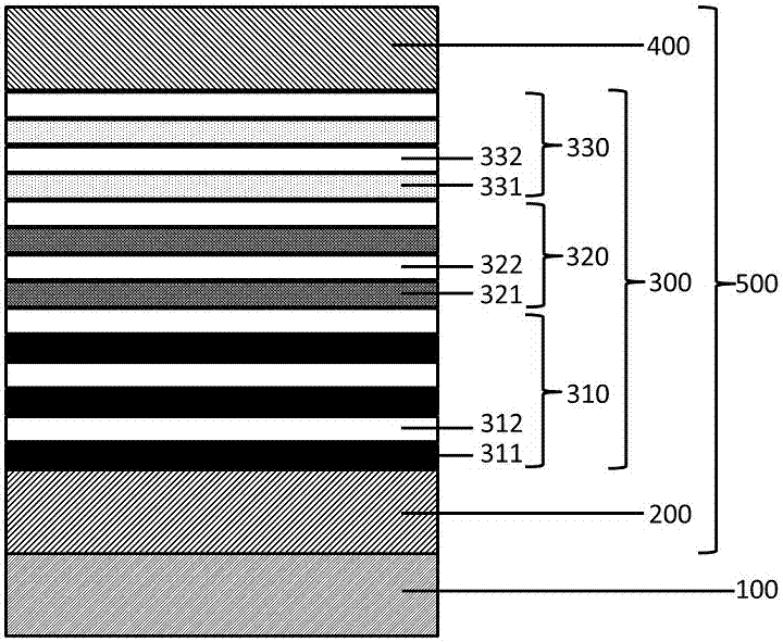
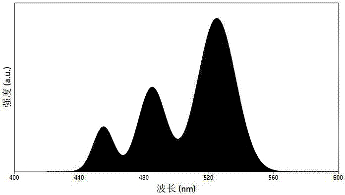
[0018] The substrate 100 adopts a silicon (Si) substrate, and the semiconductor stack 500 adopts In x Ga y Al 1-x-y N material system, n-type semiconductor layer 200 is doped with Si concentration 2×10 18 ─5×10 18 cm -3 GaN; p semiconductor layer 400 is doped with Mg concentration 1×10 20 cm -3 GaN; multi-spectral light-emitting multi-quantum well layer 300 is composed of three groups of multi-quantum well light-emitting units 310, 320 and 330 stacked and arranged sequentially from bottom to top, wherein multi-quantum well light-emitting unit 310 is composed of five periods of quantum wells 311 and quantum barriers 312. The quantum well 311 emits blue light with a wavelength of 450-460nm. The multi-quantum well light-emitting unit 320 is composed of two periods of quantum wells 321 and quantum barriers 322. The quantum well 321 emits blue light with a wavelength of 480-490nm. Well light-emitting unit 330 is made up of quantum well 331 and quantum barrier 332 of 1 period...

Embodiment 2

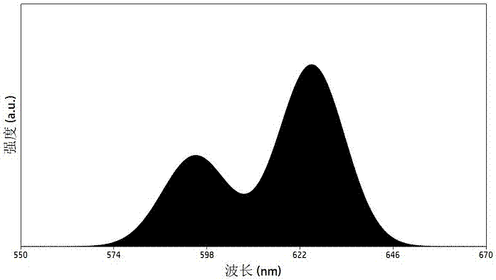
[0020] The substrate 100 is a gallium arsenide (GaAs) substrate, and the semiconductor stack 500 is In x Ga y Al 1-x-y P material system; n-type semiconductor layer 200 is n-type indium gallium aluminum phosphorus (Al x Ga y I n1-x-y P, 1≥x≥0, 1≥y≥0); the p semiconductor layer 400 is p-type indium gallium aluminum phosphorus (Al x Ga y I n1-x-y P, 1≥x≥0, 1≥y≥0); the multi-spectral light-emitting multi-quantum well layer 300 is composed of two sets of multi-quantum well light-emitting units 310 and 320 stacked in sequence, and the multi-quantum well light-emitting unit 310 consists of five periods The quantum well 311 and the quantum barrier 312 are composed of the quantum well 311, and the quantum well 311 emits orange light with a wavelength of 590-600nm. -630nm red light; the luminescent spectrum of the multi-spectral light-emitting diode structure in the present embodiment is the spectrum of red and orange two-color light synthesis, and its spectrum can be adjusted a...


PUM


Abstract

The invention discloses a multi-spectrum light-emitting diode structure, comprising: a substrate and a semiconductor stack, the semiconductor stack at least comprising an n-type semiconductor layer, a p-type semiconductor layer and a multi-spectrum light-emitting multiple quantum well layer; features Yes: the multi-spectral light-emitting multi-quantum well layer is composed of two or three sets of stacked multi-quantum well light-emitting units with different quantum well band gaps, and can emit light of two or three wavelengths at the same time, any two wavelengths The wavelength difference between the lights is λ, wherein 100nm≥λ≥10nm; the multi-quantum well light-emitting unit is a periodic structure composed of a quantum well layer and a quantum barrier layer, and the number of periods is k; the multi-quantum well light-emitting unit The luminous wavelength is determined by the forbidden band width of its quantum well, and the luminous wavelength range is 380nm─700nm. The present invention can directly emit multiple spectra in a single chip, can greatly reduce the number of chip particles used in five-primary-color white light packaging, and provides a large design window for circuit design, optical design and light mixing of lamp beads.

Description

technical field [0001] The invention relates to the technical field of semiconductor lighting, in particular to a multi-spectrum light-emitting diode structure. Background technique [0002] Light-emitting diodes (LEDs) have received widespread attention and research for their remarkable characteristics of energy saving, environmental protection, and high reliability. Today, as the energy crisis and environmental crisis are getting worse, many countries and regions have listed LED lighting technology as a national development strategy. After more than 20 years of research and hard work, LED epitaxial growth technology, LED chip manufacturing technology and LED packaging technology have all made great progress, making LEDs widely used in display screens, indicator lights, landscape lighting, automotive lights, general lighting, etc. field. [0003] At present, white LEDs for lighting are usually made in the form of "blue LED + phosphor". This form of white LED has the follo...

Claims


Application Information

Patent Timeline
Patent Type & Authority Applications(China)
IPC IPC(8): H01L33/06H01L33/04H01L33/30H01L33/26
CPCH01L33/06H01L33/04H01L33/26H01L33/30
Inventor 刘军林江风益莫春兰张建立王小兰吴小明高江东
Owner NANCHANG UNIV
Why Eureka
Try Eureka