Surface acoustic wave (SAW) device having high electromechanical coupling coefficient and high centre frequency
A surface acoustic wave device, electromechanical coupling technology, applied in electrical components, impedance networks, etc., can solve the problems of poor frequency stability of center frequency and electromechanical coupling coefficient, and achieve the effect of improving comprehensive performance, improving stability and expanding application fields
- Summary
- Abstract
- Description
- Claims
- Application Information
AI Technical Summary
Problems solved by technology
Method used
Image
Examples
Embodiment 1
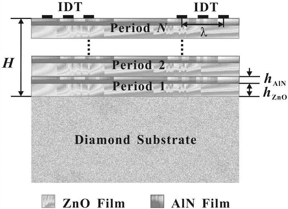
[0015] Such as figure 1 Shown based on "IDT / (AlN / ZnO) N A high-frequency surface acoustic wave device with a " / diamond" structure, which sequentially includes a base layer, a piezoelectric layer, and an interdigital transducer on the upper surface; the surface acoustic wave device uses a diamond film as a substrate, and uses AlN and ZnO thin films to be periodically laminated The structure of (AlN / ZnO) N As a piezoelectric layer, the period N of the laminated structure ranges from 2 to 5, and the thickness ratio R of the AlN film and the ZnO film is h ranges from 0.2 to 5, both AlN and ZnO thin films are c-axis preferentially oriented, and their c-axis is along the normal direction of the substrate, and the thickness of the periodic stacked structure of AlN and ZnO thin films is less than one wavelength.
[0016] The fabrication process of the surface acoustic wave device is as follows:
[0017] 1. A polished CVD diamond film is used as a substrate, the thickness of the sub...
Embodiment 2
[0022] The structure of the high-frequency surface acoustic wave device is the same as in Example 1, and its preparation process is as follows:
[0023] 1. A polished CVD diamond film is used as a substrate, the thickness of the substrate is 50 μm, and the surface roughness is 5 nm.
[0024] 2. Prepare AlN and ZnO piezoelectric films with c-axis preferential orientation by magnetron sputtering, the thicknesses of which are about 133nm and 266nm respectively, the thickness ratio of AlN and ZnO films is 0.5, and the number of cycles is 3. The thickness is 1.2 μm.
[0025] 3. An Al film with a thickness of 150 nm was prepared by vapor deposition, and an interdigital transducer with an interdigital width and spacing of 500 nm was prepared by photolithography. The IDT can be placed on the upper surface of the piezoelectric layer, or between the piezoelectric layer and the diamond substrate.
[0026] 4. The center frequency of the SAW device is 3.0GHz, and the electromechanical co...
Embodiment 3
[0028] The structure of the high-frequency surface acoustic wave device is the same as in Example 1, and its preparation process is as follows:
[0029] 1. A polished CVD diamond film is used as a substrate, the thickness of the substrate is 50 μm, and the surface roughness is 5 nm.
[0030] 2. The AlN and ZnO piezoelectric films with c-axis preferred orientation are prepared by magnetron sputtering, the thicknesses of which are 120nm and 120nm respectively, the thickness ratio of AlN and ZnO films is 1, and the number of cycles is 5, then the total The thickness is 1.2 μm.
[0031] 3. An Al film with a thickness of 150 nm was prepared by vapor deposition, and an interdigital transducer with an interdigital width and spacing of 500 nm was prepared by photolithography. The IDT can be placed on the upper surface of the piezoelectric layer, or between the piezoelectric layer and the diamond substrate.
[0032] 4. The center frequency of the SAW device is 3.5GHz, and the electro...
PUM
 Abstract
Description
Claims
Application Information
