GaN transistor and manufacturing method thereof

A technology of transistors and gallium nitride, applied in semiconductor/solid-state device manufacturing, semiconductor devices, electrical components, etc., can solve problems such as poor device performance and large ohmic contact resistance, increase device current, reduce ohmic contact resistance, The effect of improving overall performance

Inactive Publication Date: 2017-10-03
PEKING UNIV +2
View PDF2 Cites 7 Cited by
  • Summary
  • Abstract
  • Description
  • Claims
  • Application Information

AI Technical Summary

Problems solved by technology

[0005] The invention provides a gallium nitride transistor and a manufacturing method thereof, which are used to solve the technical problem of poor device performance caused by the large ohmic contact resistance of the gallium nitride transistor in the prior art

Method used


Image

  • GaN transistor and manufacturing method thereof
  • GaN transistor and manufacturing method thereof
  • GaN transistor and manufacturing method thereof

Examples


Embodiment 1

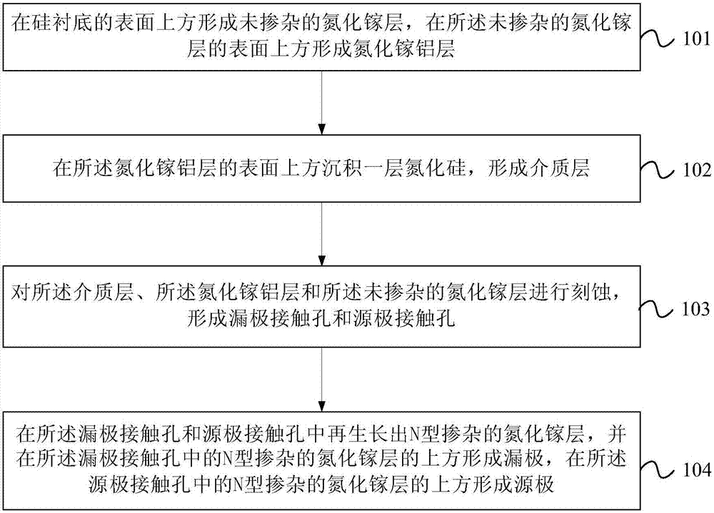
[0058] Embodiment 1 of the present invention provides a method for manufacturing a gallium nitride transistor. figure 1 It is a flowchart of a method for manufacturing a gallium nitride transistor provided in Embodiment 1 of the present invention. Such as figure 1 As shown, the method in this embodiment may include:

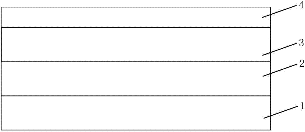
[0059] Step 101 , forming an undoped gallium nitride layer 2 on the surface of the silicon substrate 1 , and forming an aluminum gallium nitride layer 3 on the surface of the undoped gallium nitride layer 2 .

[0060] Step 102 , depositing a layer of silicon nitride on the surface of the aluminum gallium nitride layer 3 to form a dielectric layer 4 .

[0061] figure 2 It is a schematic diagram of the device structure after the dielectric layer 4 is formed in the GaN transistor manufacturing method provided in Embodiment 1 of the present invention.

[0062] Such as figure 2 As shown, a layer of gallium nitride can be deposited on the surface of the silicon su...

Embodiment 2

[0096] Embodiment 2 of the present invention provides a gallium nitride transistor. The specific structure of the gallium nitride transistor provided in this embodiment can refer to Figure 9 . Such as Figure 9 As shown, the gallium nitride transistor in this embodiment may include:

[0097] A silicon substrate 1, an undoped gallium nitride layer 2 arranged above the silicon substrate 1, an aluminum gallium nitride layer 3 arranged above the undoped gallium nitride layer, and an aluminum gallium nitride layer arranged on the said undoped gallium nitride layer a dielectric layer 4 above the aluminum gallium nitride layer 3;

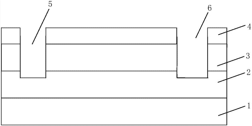
[0098] A source contact hole 6 and a drain contact hole 5 are opened in the dielectric layer 4, and both the source contact hole 6 and the drain contact hole 5 pass through the aluminum gallium nitride layer 3 and pass through Part of said undoped gallium nitride layer 2;

[0099] An N-type doped gallium nitride layer 7 is formed in the drain contact...


PUM


Abstract

The invention provides a GaN transistor and a manufacturing method thereof. The method comprises the steps of forming a non-doped GaN layer on a surface of a silicon substrate, and forming an AlGaN layer on a surface of the non-doped GaN layer; depositing a layer of silicon nitride on the surface of the AlGaN layer to form a dielectric layer; etching the dielectric layer, the AlGaN layer and the non-doped GaN layer to form a drain contact hole and a source contact hole; and growing N-type doped GaN layers in the drain contact hole and the source contact hole, forming a drain on the N-type doped GaN layer in the drain contact hole, and forming a source on the N-type doped GaN layer in the source contact hole. With the GaN transistor and a manufacturing method thereof, provided by the invention, the ohmic contact resistance can be reduced, the device current is increased, and the integral performance of the device is improved.

Description

technical field [0001] The invention relates to the technical field of semiconductors, in particular to a gallium nitride transistor and a manufacturing method thereof. Background technique [0002] Gallium Nitride (GaN) is the third generation wide bandgap semiconductor material, due to its large bandgap width, high electron saturation rate, high breakdown electric field, high thermal conductivity, corrosion resistance and radiation resistance, its application in It has strong advantages in high-voltage, high-frequency, high-temperature, high-power and radiation-resistant environmental conditions, and is considered to be the best material for short-wave optoelectronic devices and high-voltage, high-frequency and high-power devices. [0003] GaN transistors can form a two-dimensional electron gas channel with high concentration and high mobility, and at the same time have a good regulating effect on the two-dimensional electron gas channel, so it has become a research hotspo...

Claims


Application Information

Patent Timeline
IPC IPC(8): H01L21/335H01L29/778
CPCH01L29/66446H01L29/778
Inventor 刘美华孙辉林信南陈建国
Owner PEKING UNIV
Why Eureka
Try Eureka