Maskless femtosecond laser manufacturing method for super-hydrophobic and anti-reflective surface
A femtosecond laser and femtosecond laser processing technology, which is applied in the field of hydrophobic and anti-reflection material preparation, can solve the problems of high price, poor controllability of the preparation process, complex mask plate preparation, etc., and achieves low cost, good superhydrophobicity and The effect of self-cleaning properties
- Summary
- Abstract
- Description
- Claims
- Application Information
AI Technical Summary
Problems solved by technology
Method used
Image
Examples
Embodiment 1
[0036] Taking the copper base as an example below, that is, the material 7 to be processed is copper, illustrating the implementation process of a method for manufacturing a super-hydrophobic and anti-reflective surface by a femtosecond laser without a mask of the present invention, including the following steps:
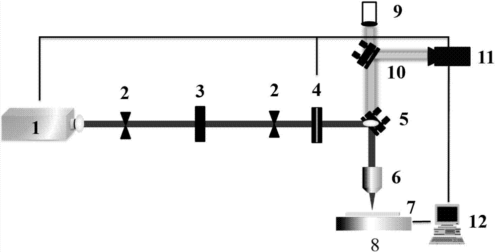
[0037] (1) build as figure 1 The femtosecond laser processing system shown; the femtosecond laser processing system consists of a femtosecond laser 1, an aperture 2, an attenuation plate 3, an optical shutter 4, and a dichromatic mirror 5; an objective lens 6, a material to be processed 7, and a six-degree-of-freedom translation stage 8 , lighting lamp 9, beam splitter 10, charge coupled device (CCD) 11, and computer 12. The femtosecond laser with a wavelength of 800nm, a pulse duration of 35fs, and a repetition rate of 1kHz is generated by the femtosecond laser 1, passes through the diaphragm 2, the attenuation plate 3, and the optical shutter 4, and is reflected b...
Embodiment 2
[0045] A method for manufacturing super-hydrophobic and anti-reflection surfaces with maskless femtosecond laser, the steps are as follows:
[0046] (1) build as figure 1 The femtosecond laser processing system shown;
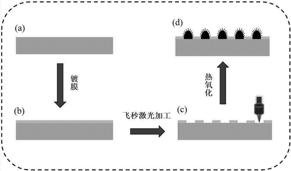
[0047] (2) if figure 2 As shown in (b), a film with a thickness of one nanometer is plated on the copper substrate by using the magnetron sputtering coating method; in this embodiment, a silicon dioxide film is plated, and the thickness of the film is 100nm. However, those skilled in the art know that in order to obtain different super-hydrophobic and anti-reflection effects, it is not limited to coating silicon dioxide films here, and this method can be used to coat gold, silver and other thin films of different thicknesses;
[0048] (3) if figure 2 As shown in (c), in air, a femtosecond laser is used to selectively ablate and remove silicon dioxide on a copper substrate coated with a silicon dioxide film to process a linear array structure. However, tho...
PUM
| Property | Measurement | Unit |
|---|---|---|
| thickness | aaaaa | aaaaa |
| thickness | aaaaa | aaaaa |
| contact angle | aaaaa | aaaaa |
Abstract
Description
Claims
Application Information


