Solid light microchannel array panel and preparation method thereof

An array panel and optical channel technology, applied in the field of optical components, can solve problems such as difficult to achieve optical effects, unfavorable packaging and use, and harsh environmental requirements, and achieve the effects of favorable packaging and use, low cost, and low cleanliness requirements

Active Publication Date: 2017-10-24
GUANGZHOU HONSUN OPTOELECTRONICS
View PDF8 Cites 6 Cited by
  • Summary
  • Abstract
  • Description
  • Claims
  • Application Information

AI Technical Summary

Problems solved by technology

[0005] 1) The length-to-diameter ratio of through holes processed by these manufacturing methods is generally less than 30, and there are quality defects such as blind holes and tapered holes, making it difficult to achieve ideal optical effects
[0006] 2) The processing efficiency is low. Due to the limitation of the depth of drilling, etching, acid dissolution or cleaning, these technical solutions can only realize sheet processing, the processing technology is complicated, and the processing process is required to be completed in a relatively clean environment. In order to prevent the through holes from being blocked by dust, the environmental requirements for packaging and use are almost strict; in the process of processing, it is necessary to adjust the opening ratio of the array structure by adjusting the thickness of the tube, which is not flexible enough
[0007] 3) No matter whether the products produced by these technical solutions are metal, semiconductor or inorganic materials, the strength of the products will be seriously reduced after the through holes are filled, which is not conducive to subsequent packaging and use

Method used


Image

  • Solid light microchannel array panel and preparation method thereof
  • Solid light microchannel array panel and preparation method thereof
  • Solid light microchannel array panel and preparation method thereof

Examples


preparation example Construction

[0070] refer to Figure 7 , a method for preparing a solid optical microchannel array panel, comprising the following steps:

[0071] drawing the first light-transmitting medium material rod and the opaque base material rod into thin rods of the first light-transmitting medium material and the thin rods of the opaque base material;

[0072] Arranging and combining the thin rods of the first light-transmitting medium material and the thin rods of the opaque base material to form a composite rod, the first rods of the light-transmitting medium material being wrapped by the adjacent rods of the opaque base material;

[0073] Draw a primary composite rod to make a primary composite channel filament;

[0074] According to the size requirements of the optical channel to be prepared, the primary composite channel wire is made into a rough composite wire rod of the size required by the solid optical microchannel array panel;

[0075] Fusing the blank composite wire rod into a blank ...

no. 1 example

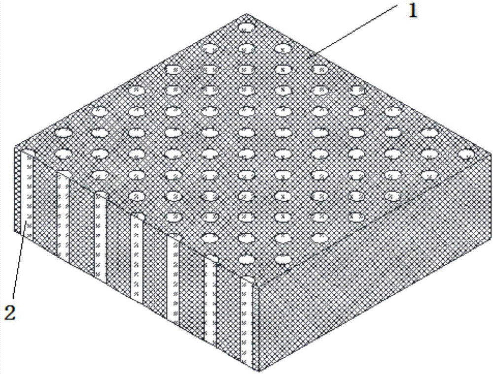
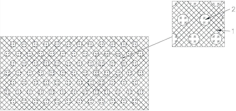
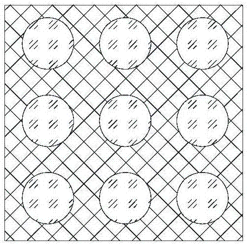
[0113] Aiming at the problems caused by the non-solid structure of through holes in the existing microhole array structure, the present invention proposes a new solid optical microchannel array panel. Such as figure 1 and 2 As shown, the array panel mainly includes a light-tight base 1 and a plurality of light-transmitting channels 2 .

[0114] Wherein, the light-transmitting channel 2 uses a transparent optical medium (such as transparent glass, transparent plastic, etc.) as the light channel to allow light to pass through. In addition, the light-transmitting channel 2 is a solid light channel.

[0115] The opaque substrate 1 uses opaque or light-absorbing materials (such as opaque glass, opaque plastic, etc.) as spacers to isolate the light between the light-transmitting channels 2 .

[0116] Such as figure 1 and figure 2 As shown, each light-transmitting channel 2 is arranged in parallel, and the light-impermeable matrix 1 is filled between each light-transmitting cha...

no. 2 example

[0120] Such as Figure 9-12 As shown, the transparent glass rod 202 made of transparent glass with the second light-transmitting medium rod, the black glass tube 201 made of black glass as the opaque base material tube, and the first thin filler wire made of black glass The black filament 203 and the second thin filler filament are black filament 204 made of black glass as an example, assuming that the optical channel size of the primary composite channel filament does not meet the optical channel size requirements to be prepared, the method of fusing the blank rod is vacuum drawing Manufacturing method, then adopt the tube-and-rod method of the present invention to prepare the technological process of solid optical microchannel array panel as follows:

[0121] The first step: use the rod tube to pull the single-channel thin rod.

[0122] The specific realization process of adopting rod-tube farad single-channel thin rods is as follows: according to the designed process param...


PUM


Abstract

The invention discloses a solid light microchannel array panel and a preparation method thereof. The panel comprises a panel body, wherein the panel body comprises light-tight base bodies and multiple light-permeable channels; the light-tight base bodies are arranged among the light-permeable channels which are solid light channels. The preparation method comprises steps as follows: first light-permeable medium material bars and light-tight base body material bars are drawn into thin first light-permeable medium material bars and thin light-tight base body material bars; the thin first light-permeable medium material bars and the thin light-tight base body material bars are arranged and combined into primary composite bars; the primary composite bars are drawn into primary composite channel filaments; the primary composite channel filaments are made into blank composite filament bars; the blank composite filament bars are melt to form blank bars; the blank bars are subjected to follow-up processing, and the solid light microchannel array panel is obtained. The light channels have a large length-diameter ratio, the optical effect is good, requirements for environments in the packaging and use processes are low, and the panel is high in strength and efficiency, low in cost, flexible and capable of being widely applied to the field of optical elements.

Description

technical field [0001] The invention relates to the field of optical components, in particular to a solid optical microchannel array panel and a preparation method thereof. Background technique [0002] With the development of binary optics, MEMS and fingerprint acquisition technology, optical components with microhole array structure have been widely used, such as microhole aperture, photon sieve, laser microhole resonator, silicon microchannel plate, microchannel Plate (MCP), microhole array collimator for UnderDisplay mobile fingerprint recognition technology, etc. [0003] The essential role of the microhole array structure in optical components is to provide mutually isolated optical channels. [0004] At present, the methods for making similar microhole array structural elements at home and abroad include laser drilling method, photolithography method, microchannel plate method, light-assisted electrochemical etching method, etc. The same idea of ​​the channel has th...

Claims


Application Information

Patent Timeline
Patent Type & Authority Applications(China)
IPC IPC(8): C03B37/025C03B37/028C03B37/14
CPCC03B37/025C03B37/028C03B37/14C03B2203/10C03B2205/08C03B2203/40Y02P40/57
Inventor 何相平叶灵西吴若萍李建杰王斌
Owner GUANGZHOU HONSUN OPTOELECTRONICS
Why Eureka
Try Eureka