Varactor structure used in flash memory circuit and manufacture method thereof

A varactor diode and flash memory technology, which is applied in the direction of circuits, semiconductor/solid-state device manufacturing, electrical components, etc., can solve the problem of chip area reduction and achieve the effect of expanding and improving capacitance

Active Publication Date: 2017-11-14
SHANGHAI HUALI MICROELECTRONICS CORP
View PDF7 Cites 1 Cited by
  • Summary
  • Abstract
  • Description
  • Claims
  • Application Information

AI Technical Summary

Problems solved by technology

However, increasing the capacitor area in a limited chip area will cause additional work such as redesign of other circuit designs, and the increased area is not conducive to the continuous reduction of chip area. Therefore, the industry needs to design a capacitor that can meet the needs of large-capacity capacitors. Varactor diodes used in flash memory circuits that can take into account the trend of chip miniaturization

Method used


Image

  • Varactor structure used in flash memory circuit and manufacture method thereof
  • Varactor structure used in flash memory circuit and manufacture method thereof
  • Varactor structure used in flash memory circuit and manufacture method thereof

Examples


Embodiment 1

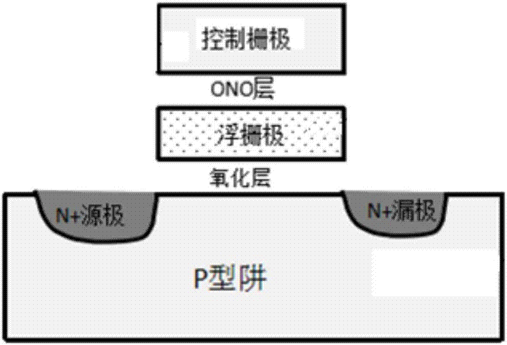
[0047] see Figure 4 , Figure 4 It is a schematic diagram of a preferred embodiment of the varactor diode structure used in the flash memory circuit of the present invention. The varactor diode includes a substrate 1, a first insulating layer 2 formed on the substrate 1, a floating gate 3 formed on the first insulating layer 2, and a control gate opposite to the floating gate 3 4, and the second insulating layer 5 formed between the floating gate 3 and the control gate 4, the first insulating layer 2 is also called a tunnel oxide layer, and a source and a drain are formed on the substrate 1.

[0048] In this embodiment, preferably, the material of the first insulating layer 2 may be silicon dioxide, and the second insulating layer 5 may be a silicon oxide / silicon nitride / silicon oxide (ONO) structure.

[0049] The floating gate 3 is separately drawn out as a pole plate, image 3 It illustrates a lead-out method provided by the embodiment of the present invention, that is, ...

Embodiment 2

[0054] see Figure 5 , Figure 5 It is a schematic diagram of another preferred embodiment of the varactor diode structure used in the flash memory circuit of the present invention.

[0055] The varactor diode structure used in the flash memory circuit provided by this embodiment can include all the structural elements in the flash memory transistor structure of the first embodiment, the difference is that the floating gate 3 of the varactor diode structure in the first embodiment can be viewed from its side Leading out, in the embodiment of the present invention, the leading out line of the floating gate 3 needs to pass through the second insulating layer 5 and the control gate 4 . Its formation process includes:

[0056] On the control grid 4 and the second insulating layer 5, vertically connected through holes are respectively formed, and a contact hole is formed in the through hole through the insulating layer to connect with the floating gate 3, thereby leading out the ...


PUM


Abstract

The invention provides a varactor structure used in a flash memory circuit and a manufacture method thereof. The varactor structure comprises a substrate, a first insulating layer formed on the substrate, a floating gate formed on the first insulating layer, a control gate arranged opposite to the floating gate, and a second insulating layer formed between the floating gate and the control gate. A source and a drain are formed on the substrate. A first connection wire separately led out from the floating gate and is used as a polar plate of the capacitor of the varactor. The source lead out wire, the drain lead out wire and the lead out wire of the control gate are electrically connected together to form a second connection wire, and the second connection wire is used as the other polar plate of the capacitor of the varactor. The first insulating layer and the second insulating layer are used as the dielectric layer of the capacitor of the varactor. The varactor used in the flash memory circuit can meet the demand of a large-capacity capacitor, and can take the trend of chip miniaturization into account.

Description

technical field [0001] The invention belongs to the technical field of semiconductors, and relates to a varactor diode structure used in a flash memory circuit and a manufacturing method thereof. Background technique [0002] Varactor Diodes, also known as "variable reactance diodes", are diodes made using the dependence and principle of PN junction capacitance (barrier capacitance) and its reverse bias voltage. When a forward bias is applied, a large amount of current is generated, the depletion region of the PN (positive and negative) junction becomes narrower, the capacitance becomes larger, and a diffusion capacitance effect occurs; when a reverse bias is applied, a transition capacitance effect occurs , but because there will be a leakage current when the forward bias is applied, so the reverse bias is supplied in the application, such as figure 1 shown. [0003] Varactor diodes, also known as voltage-controlled varactors, are semiconductors that change the junction c...

Claims


Application Information

Patent Timeline
IPC IPC(8): H01L29/93H01L21/329
CPCH01L29/66174H01L29/93
Inventor 田志钟林建殷冠华陈昊瑜
Owner SHANGHAI HUALI MICROELECTRONICS CORP
Why Eureka
Try Eureka