Semiconductor light-emitting element and preparation method thereof

A technology for light-emitting components and semiconductors, applied in semiconductor devices, electrical components, circuits, etc., can solve the problem of reducing the luminous efficiency of semiconductor components, and achieve the effect of improving the hole injection effect, improving the luminous efficiency, and reducing the overflow of electrons.

Active Publication Date: 2017-11-24
ANHUI SANAN OPTOELECTRONICS CO LTD
View PDF3 Cites 9 Cited by
  • Summary
  • Abstract
  • Description
  • Claims
  • Application Information

AI Technical Summary

Problems solved by technology

[0003] However, when growing the P-type semiconductor layer, because of its growth temperature and conditions, the doping material Mg of the P-type semiconductor is easily diffused from the P-type semiconductor layer into the quantum well structure layer, which affects the material quality of the potential well layer in the quantum well structure layer. , leading to a decrease in the luminous efficiency of semiconductor components. Therefore, we urgently need to find a preparation method and a semiconductor structure to suppress the diffusion of Mg and prevent the luminous efficiency of semiconductor components from decreasing.

Method used


Image

  • Semiconductor light-emitting element and preparation method thereof
  • Semiconductor light-emitting element and preparation method thereof

Examples


Embodiment Construction

[0024] In the following paragraphs the invention is described more specifically by way of example with reference to the accompanying drawings. Advantages and features of the present invention will be apparent from the following description and claims. It should be noted that all the drawings are in a very simplified form and use imprecise scales, and are only used to facilitate and clearly assist the purpose of illustrating the embodiments of the present invention.

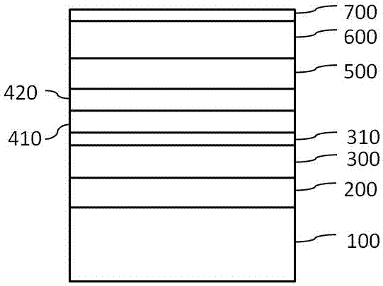
[0025] See attached figure 1 , the bright semiconductor light-emitting element provided by the present invention, which includes a substrate 100 and an N-type layer 200, a multi-quantum well structure layer 300, a final barrier layer 310, an electron blocking layer 500, and a P-type layer 600 sequentially located on the substrate 100 and the P-type contact layer 700 . The multi-quantum well structure layer 300 includes alternately stacked barrier layers and potential well layers, wherein the substrate 100 can be...


PUM


Abstract

The present invention belongs to the semiconductor technology field, in particular to a semiconductor light-emitting element and a preparation method thereof. According to the present invention, a first cover layer and a second cover layer of high energy levels grow at a low temperature between a final barrier layer and an electron barrier layer, the first cover layer is an un-doped layer growing relatively at the low temperature and is used to reduce the situation that the P-type impurities diffuse to a multi-quantum well structural layer, so that the luminescence efficiency reduces, and the second cover layer is a hole injection layer, is doped with the P-type impurities of high concentration to improve a hole injection effect. Meanwhile, by utilizing the higher energy levels of the first cover layer and the second cover layer, the electron overflow is reduced effectively, and the luminescence efficiency of the semiconductor element is improved.

Description

technical field [0001] The invention belongs to the technical field of semiconductors, and in particular relates to a semiconductor light-emitting element and a preparation method thereof. Background technique [0002] GaN-based light-emitting diodes include a P-N junction that converts electrical energy into light energy, and an N-type semiconductor layer for providing electrons and a P-type semiconductor layer for providing holes. When a forward voltage is applied to the light-emitting diode, the N-type semiconductor layer Electrons of the semiconductor layer are combined with holes of the P-type semiconductor layer, so that energy corresponding to an energy gap between a conduction band and a valence band may be released. The energy is mainly manifested as heat or light, and the light emitting diode emits the energy as light. [0003] However, when growing the P-type semiconductor layer, because of its growth temperature and conditions, the doping material Mg of the P-ty...

Claims


Application Information

Patent Timeline
Patent Type & Authority Applications(China)
IPC IPC(8): H01L33/02H01L33/14H01L33/00
CPCH01L33/0075H01L33/02H01L33/14H01L33/06H01L33/32
Inventor 蓝永凌蔡吉明林兓兓张家宏
Owner ANHUI SANAN OPTOELECTRONICS CO LTD
Why Eureka
Try Eureka