

Doped perovskite solar cell and method for preparing same
A solar cell and perovskite technology, applied in circuits, photovoltaic power generation, electrical components, etc., can solve the problems of low battery efficiency and hindering charge transmission, and achieve the effects of suitable industrial production, improved photoelectric performance, and easy preparation
- Summary
- Abstract
- Description
- Claims
- Application Information
AI Technical Summary
Problems solved by technology
Method used
Image

Examples
Embodiment 1
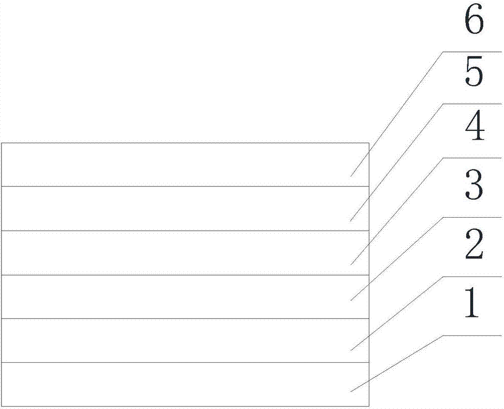
[0039] in CH 3 NH 3 PB 3 For the perovskite absorber layer, PC 61 BM is the electron transport layer, BCP is the buffer layer, and Ag is the metal electrode. The specific preparation steps are as follows:
[0040] A. Cleaning of FTO conductive glass: Use glass cleaner, deionized water, high-purity water, absolute ethanol, and acetone to ultrasonically clean FTO conductive glass for 15-20 minutes, then blow dry with nitrogen for use;
[0041] B. NiO x Preparation of the hole transport layer: using nickel acetylacetonate and magnesium acetate as raw materials, prepare the first precursor solution of nickel acetylacetonate containing magnesium acetate, wherein the molar concentration of nickel acetylacetonate is 0.01-0.05mol / L, doped atoms The ratio is: Mg:Ni=(1-2):10, with acetonitrile as the solvent; put the above-mentioned cleaned FTO glass with the conductive side facing up, place it on a hot plate at a temperature of 500-600°C, and spray the above-mentioned Precursor. Af...
Embodiment 2
[0051] Reference example one cleaning FTO glass, preparing NiO x hole transport layer. This example uses CH 3 NH 3 PB 2.4 Cl 0.6 It is the perovskite absorbing layer. CH 3 NH 3 I, PbI 2 and PbCl 2 Add it into the DMF solution according to the molar ratio of 1:0.7:0.3, prepare the second precursor solution with a molar concentration of 0.5-1.5mol / L, and then add MoS 2 Powder, MoS 2 The amount of powder added: 0.02-0.04mg per milliliter of the second precursor solution will be added, and then stirred and dissolved at 75-80°C for 2-3h to form CH 3 NH 3 PB 2.4 Cl 0.6 Perovskite Precursor. The above-mentioned perovskite precursor solution was coated on NiO by slit coating. x On the hole transport layer, then anneal at 80-100°C for 10-30min to form a 400-500nm perovskite absorption layer; then coat PC by slot coating 71 Chlorobenzene solution of BM (20mg / mL), annealed at 100°C for 10min to form PC with a thickness of 50-80nm 71 BM electron transport layer; the abov...
Embodiment 3
[0057] Reference example one cleaning FTO glass, preparing NiO x hole transport layer. This example uses CH 3 NH 3 PB 2.4 Br 0.6 It is the perovskite absorbing layer. CH 3 NH 3 I, PbI 2 and PbBr 2 Add it into the DMF solution according to the molar ratio of 1:0.7:0.3, prepare the second precursor solution with a molar concentration of 0.5-1.5mol / L, and then add MoS 2 powder (same as above), then stirred and dissolved at 75-80°C for 2-3h to form CH 3 NH 3 PB 2.4 Br 0.6 Perovskite Precursor. The above perovskite precursor solution was coated on NiO by screen printing. x On the hole transport layer, then anneal at 80-100°C for 10-30min to form a 400-500nm perovskite absorption layer; then coat bis-PC by screen printing 61 Chlorobenzene solution of BM (20mg / mL), annealed at 100°C for 10min to form bis-PC with a thickness of 50-80nm 61 BM electron transport layer; the above glass substrate was transferred to a vacuum evaporation chamber until the pressure reached 1...
PUM
| Property | Measurement | Unit |
|---|---|---|
| Film thickness | aaaaa | aaaaa |
| Thickness | aaaaa | aaaaa |
| Thickness | aaaaa | aaaaa |
Abstract
Description
Claims
Application Information