Broad-band gap semiconductor vertical double diffusion metal oxide semiconductor field effect transistor having composite dielectric layer and manufacturing method thereof

An oxide semiconductor, vertical double diffusion technology, applied in semiconductor/solid-state device manufacturing, semiconductor devices, electrical components, etc., can solve the problems of increased device conduction loss and increased on-resistance

Active Publication Date: 2017-12-05
XIDIAN UNIV
View PDF2 Cites 5 Cited by
  • Summary
  • Abstract
  • Description
  • Claims
  • Application Information

AI Technical Summary

Problems solved by technology

However, in the field of high-voltage applications of power devices, as the breakdown voltage of the device increases, the thickness of the power VDMOS epitaxial layer increases continuously, and the doping concentrati

Method used


Image

  • Broad-band gap semiconductor vertical double diffusion metal oxide semiconductor field effect transistor having composite dielectric layer and manufacturing method thereof

Examples


Embodiment Construction

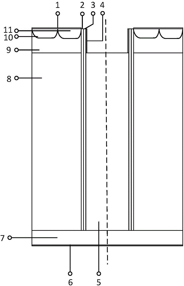
[0043] Such as figure 1 As shown, the vertical double-diffused metal oxide semiconductor field effect transistor based on the wide bandgap semiconductor compound dielectric layer includes:

[0044] The substrate drain region 7 of the wide bandgap semiconductor material, the doping concentration is determined according to the growth conditions and doping process of the wide bandgap semiconductor material, and the typical value range is 1×10 12 cm -3 ~1×10 15 cm -3 ;

[0045] A drift region 8 formed by an epitaxial layer on the substrate;

[0046] a base region 9 formed by doping on the drift region;

[0047] Etching a trench on the base region, the trench goes down through the drift region to the substrate drain region;

[0048] The gate insulating layer 2 formed on the side wall of the trench has a thickness of 0.02-0.1 μm;

[0049] Oxygen-doped semi-insulating polysilicon layer 3 deposited outside the gate insulating layer; the thickness of the semi-insulating polysili...


PUM

PropertyMeasurementUnit
Widthaaaaaaaaaa
Thicknessaaaaaaaaaa
Thicknessaaaaaaaaaa

Abstract

The invention provides a broad-band gap semiconductor vertical double diffusion metal oxide semiconductor field effect transistor having a composite dielectric layer and a manufacturing method thereof. The device is characterized in that the composite dielectric layer is formed by a semi-insulation polysilicon layer (SIPOS) and a high dielectric constant (High K) dielectric layer at a drift region side wall below a device gate electrode. When the device is turned off, the SIPOS column and the High K dielectric layer have uniform electric fields, electric distribution in the drift region of the device is made to be uniform through electric field modulation, moreover, exhaust of the drift region is commonly facilitated by the SIPOS column and the High K dielectric layer, exhaust capability of the device drift region is substantially improved, drift region doping concentration of the device is made to increase, and conduction resistance is reduced; when the device is turned on, the side wall of the drift region has multiple carrier accumulation layers, and conduction resistance of the device is reduced further.

Description

technical field [0001] The invention relates to the field of semiconductor devices, in particular to a trench (Trench) type vertical double-diffused metal oxide semiconductor field effect transistor. Background technique [0002] Wide bandgap semiconductor materials have the characteristics of large band gap, high critical breakdown electric field, high thermal conductivity and high electron saturation drift velocity, so they have very broad application prospects in the field of high-power, high-temperature and high-frequency power electronics. At present, among the field effect transistors based on SiC, a typical wide-bandgap semiconductor, the vertical double-diffused metal-oxide-semiconductor field effect transistor (VDMOS) is one of the widely studied objects. In 1985, a trench (Trench) MOS structure was proposed by D.Ueda et al. The U-shaped groove structure makes the conduction channel of the device change from horizontal to vertical, which effectively eliminates the ...

Claims


Application Information

Patent Timeline
IPC IPC(8): H01L29/78H01L21/336
CPCH01L29/66734H01L29/7813
Inventor 段宝兴曹震吕建梅师通通杨银堂
Owner XIDIAN UNIV
Why Eureka
Try Eureka