
A kind of preparation method of composite anti-plating mask

An anti-plating and masking technology, which is applied in the manufacture of circuits, electrical components, semiconductors/solid-state devices, etc., can solve problems such as degumming, production failure, and easy dissolution of photoresist, and achieve high line precision, simple method, and graphic resolution high rate effect

Active Publication Date: 2020-01-14
NO 20 RES INST OF CHINA ELECTRONICS TECH GRP
View PDF4 Cites 0 Cited by
  • Summary
  • Abstract
  • Description
  • Claims
  • Application Information

AI Technical Summary

Problems solved by technology

The mature photoresist products on the market have high viscosity and are suitable for spin coating. If spray coating is required, the photoresist must be diluted. There are a lot of solvents in the diluted photoresist, and the chemical stability and physical stability are poor.
Diluted photoresist is used as the anti-electroplating film. In the subsequent electroplating process, the corrosion resistance of the electroplating solution is poor, and the photoresist is easy to dissolve and degumming occurs, resulting in fuzzy circuit graphics and production failure.
[0004] At present, there are two types of methods to solve this problem. One is to use photoresist resistant to electroplating solution, but the photoresist resistant to electroplating solution needs to be sprayed when coating complex surfaces, and the photoresist needs to be diluted. After the resist is diluted, there is still the problem of poor corrosion resistance to the plating solution; another method is to etch the seed layer first, pattern the seed layer and then electroplate without an anti-electroplating film, but the electroplating of isolated patterns needs to introduce a process line, high density It is not easy to remove complex circuit process lines in the later stage. In addition, there is no electroplating film plating, and there is no restriction of electroplating film. When the circuit is electroplated, metal ions will expand around the pattern, resulting in poor pattern accuracy and low bonding force with the substrate.

Method used


Image

  • A kind of preparation method of composite anti-plating mask

Examples


preparation example Construction

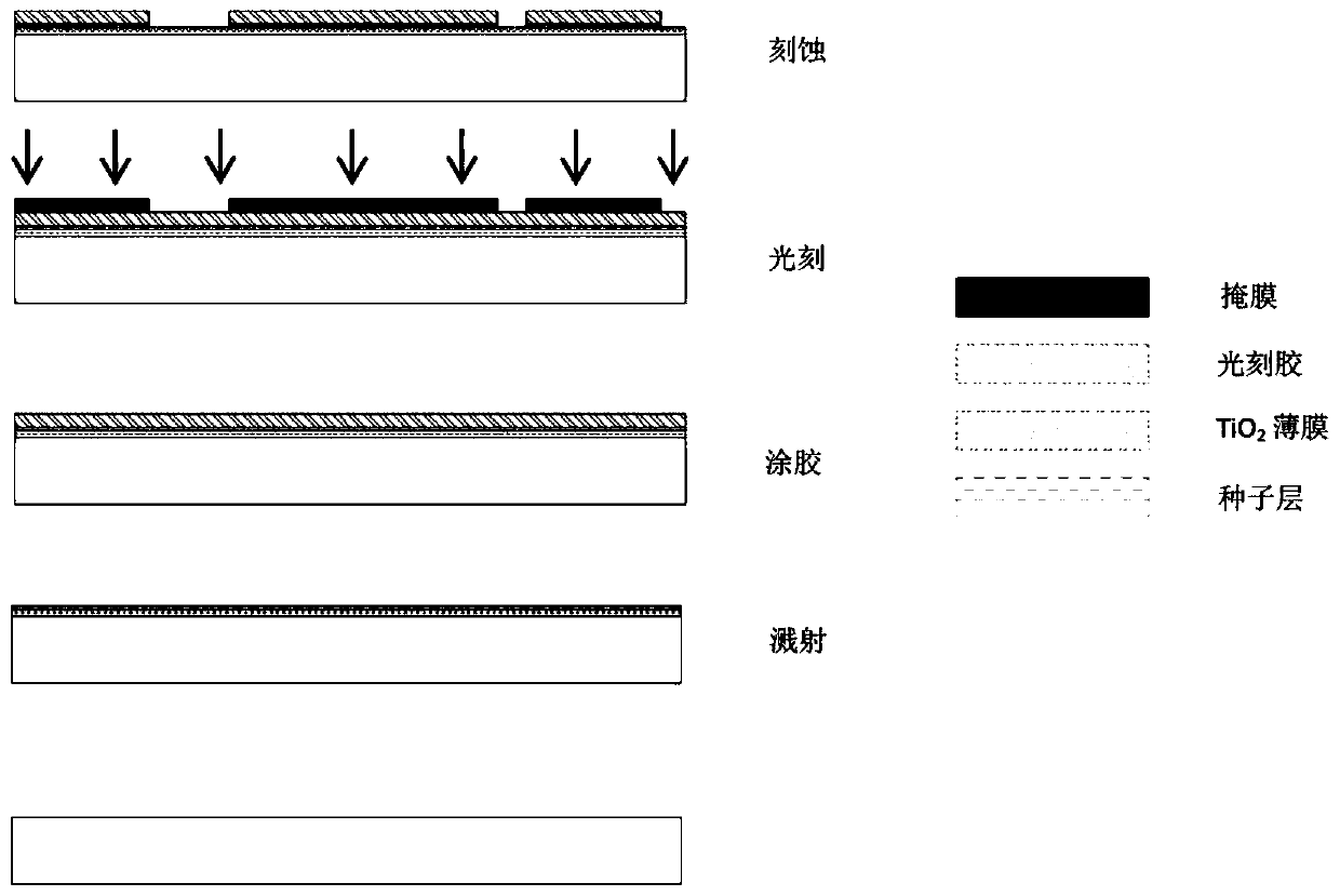
[0025] A kind of preparation method of composite anti-plating mask provided by the invention comprises the following steps:

[0026] (1) Sputtering

[0027] The cleaned Al 2 o 3 The ceramic substrate is placed in the magnetron sputtering coating chamber, and Cr, Cu, TiO are sequentially sputtered 2 Three-layer film, in which Cr film thickness is 50-100nm, Cr and Cu gradient transition layer thickness is 50-100nm, Cu film thickness is 400-500nm, TiO 2 The film thickness is 200-300nm. The sputtering power was 300W, and the Ar flow rate was 100 sccm.

[0028] (2) spray glue

[0029] Place the ceramic substrate with the metal / oxide film deposited in the previous step in the glue sprayer, and spray the diluted positive photoresist. The positive photoresist is AZ4620 from Anzhi Company, and the diluent is methyl ethyl ketone and PGMEA. The degree is based on the fact that the viscosity of the photoresist is less than 0.03 Pa·S, and the rotation speed of the substrate is 50 rpm...

Embodiment 1

[0056] A preparation method of a composite anti-plating mask, comprising the following steps:

[0057] (1) Sputtering

[0058] Place the cleaned ceramic substrate in the magnetron sputtering coating chamber, and the chamber is evacuated to 3.7×10 -4 Pa, turn on the heating, bake and dehumidify the substrate, the baking time and temperature are 250°C and 30min, respectively, and start sputtering deposition of Cr, Cu, TiO 2 Three-layer film, in which Cr and Cu are the circuit seed layer, co-sputtered Cr / Cu interlayer between Cr and Cu, TiO 2 For anti-plating film. Sputtering power is 300W, Ar flow rate is 100sccm, Cr film thickness is 60nm, Cr and Cu gradient transition layer thickness is 50nm, Cu film thickness is 400nm, TiO 2 The film thickness is 200 nm.

[0059] (2) spray glue

[0060] Place the ceramic substrate deposited with the seed layer in the glue sprayer, and spray the diluted positive photoresist. The photoresist is AZ4620 from Anzhi Company, and the diluent is...

Embodiment 2

[0070] A preparation method of a composite anti-plating mask, comprising the following steps:

[0071] (1) Sputtering

[0072] Place the cleaned ceramic substrate in the magnetron sputtering coating chamber, and the chamber is vacuumed to 3.5×10 -4 Pa, turn on the heating, bake and dehumidify the substrate, the baking time and temperature are 250°C and 30min, respectively, and start sputtering deposition of Cr, Cu, TiO 2 Three-layer film, in which Cr and Cu are the circuit seed layer, co-sputtered Cr / Cu interlayer between Cr and Cu, TiO 2 For anti-plating film. Sputtering power is 300W, Ar flow rate is 100sccm, Cr film thickness is 50nm, Cr and Cu gradient transition layer thickness is 50nm, Cu film thickness is 450nm, TiO 2 The film thickness is 220 nm.

[0073] (2) spray glue

[0074] Place the ceramic substrate deposited with the seed layer in the glue sprayer, and spray the diluted positive photoresist. The photoresist is AZ4620 from Anzhi Company, and the diluent is ...


PUM

PropertyMeasurementUnit
thicknessaaaaaaaaaa
thicknessaaaaaaaaaa
thicknessaaaaaaaaaa

Abstract

The invention provides a preparation method of a composite anti-electroplating mask. A TiO2 and photoresist composite film is used as an anti-electroplating film. A composite film is prepared by using the photoresist by means of sputtering, photoetching and etching. The method is simple and does not require additional process equipment. The composite film retains the high graphics resolution and high line precision of the photoresist as the anti-electroplating film, and overcomes the unfavorable characteristics of the photoresist unresisting to the corrosion of an electroplating solution. The method solves a problem that a photoresist mask is liable to be dissolved and eroded in the electroplating solution, introduces a TiO2 film to form the composite anti-electroplating mask with the photoresist, and determines the thickness of the TiO2 film and the photoresist and a preparation process and process parameters.

Description

technical field [0001] The invention relates to a thin film circuit preparation process. Background technique [0002] Thin-film circuits are made of overlapping conductors, passive devices and insulating dielectric films on a polished substrate by using film-forming processes such as vacuum coating and electroplating, and patterning technologies such as ultraviolet lithography, wet etching, and dry etching. Multilayer interconnection circuit structure. Compared with other types of circuits, thin-film circuits have high interconnection density and high line precision, can realize small hole metallization, integrate passive components such as resistors, capacitors and inductors, and manufacture high-power circuits. The entire package structure has system-level functions It has a wide range of applications in microwave and millimeter wave circuits in airborne, spaceborne and aerospace fields, and is a very potential microwave circuit substrate technology. [0003] Usually, t...

Claims


Application Information

Patent Timeline
Patent Type & Authority Patents(China)
IPC IPC(8): H01L21/027H01L21/203H01L21/70
CPCH01L21/0274H01L21/2036H01L21/70
Inventor 陈帅
Owner NO 20 RES INST OF CHINA ELECTRONICS TECH GRP
Learn More