Prepressing type PCB hole residue removal device

A PCB board and pre-pressing technology, applied in the field of mechanical devices, can solve the problems of secondary pollution of waste chips, long reaction time, low efficiency, etc., so as to improve the yield rate of PCB boards, prevent secondary pollution, and prevent hole wall damage. Effect

Active Publication Date: 2017-12-22
SUZHOU WUTONG ELECTRONICS CO LTD
View PDF7 Cites 2 Cited by
  • Summary
  • Abstract
  • Description
  • Claims
  • Application Information

AI Technical Summary

Problems solved by technology

[0002] Printed circuit board, also known as PCB board, is the support body of electronic components and the carrier of electrical connection of electronic components. The manufacturing process of PCB board is complicated. The general process is: cutting, drilling, electroless copper (PTH) Copper plating and electroplating, pattern transfer (circuit), pattern electroplating (second copper) and protective tin plating, etching (SES), intermediate inspection, solder mask (Solder Mask), printing characters, metal surface treatment, finished product molding, electrical testing, Appearance inspection (FQC / OQA), packaging and shipment, after the PCB board is drilled, there is a certain probability that slag will adhere to the PCB drill hole. Therefore, the PCB board needs to be desmeared before copper sinking. Soaking the PCB board in the medicine tank to remove the smear not only takes a long time, but also requires repeated desmearing actions to completely remove the smear, which is inefficient. You can also remove the smear manually. It is necessary to clamp the PCB board every time, every time a PCB board is processed, it needs to be clamped once, which takes a long time and the efficiency is relatively low.

Method used


Image

  • Prepressing type PCB hole residue removal device
  • Prepressing type PCB hole residue removal device
  • Prepressing type PCB hole residue removal device

Examples


Embodiment Construction

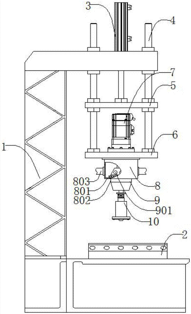
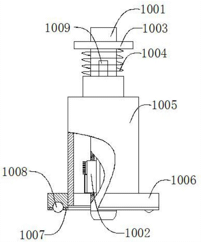
[0035] like figure 1 , figure 2 , image 3As shown, a pre-pressed PCB board hole slag removal device includes a frame 1, a placement mold 2, a cylinder 3, a guide rod 4 arranged symmetrically along the cylinder 3, an upper pallet 5, a lower pallet 6, an adjustment Speed ​​motor 7, bellows 8, collet 9, pre-pressing drill mechanism 10, described placement mold 2 is positioned at frame 1 lower end, described placement mold 2 is connected with frame 1 screw thread, and described cylinder 3 is positioned at machine The upper end of the frame 1, the cylinder 3 is threadedly connected with the frame 1, the guide rod 4 runs through the frame 1, the guide rod 4 is connected with the frame 1 with a gap, and the upper supporting plate 5 is located on the cylinder 3 The lower end is penetrated by the guide rod 4, the upper supporting plate 5 is threadedly connected with the cylinder 3 and connected with the guide rod 4, the lower supporting plate 6 is located at the lower end of the gu...


PUM


Abstract

The invention discloses a prepressing type PCB hole residue removal device. The prepressing type PCB hole residue removal device comprises a rack, a placement mold, an air cylinder, guide rods symmetrically arranged along the air cylinder, an upper supporting board, a lower supporting board, a speed adjusting motor, an air bellow, a chuck and a prepressing drilling tool mechanism. A PCB to be subjected to residue clearing is placed in the placement mold, the air cylinder pushes the upper supporting board to move downwards, and therefore the prepressing drilling tool mechanism is pushed to move downwards to tightly press the PCB; then the speed adjusting motor works, tool bits arranged on drilling tool mechanism bodies smash and remove residues attached in a hole, brushes sweep the hole wall machined by the tool bits, and therefore the residues are removed; and an air pipe carries out extraction in the air bellow to form negative pressure, and free waste chips pass through a hollow sleeve pipe and a chip outlet hole in sequence to enter the air bellow and then are discharged by the air pipe. The device is simple in structure, and residues and chips attached to the inner wall of the hole of the PCB can be effectively removed; environment friendliness is achieved, and the free waste chips can be collected to prevent secondary contamination of the waste chips; and meanwhile, prepressing can be carried out automatically, hole wall damage caused by PCB deformation can be avoided, and the yield of the PCB can be increased.

Description

technical field [0001] The invention relates to a mechanical device, in particular to a pre-pressed PCB hole slag removal device. Background technique [0002] Printed circuit board, also known as PCB board, is the support body of electronic components and the carrier of electrical connection of electronic components. The manufacturing process of PCB board is complicated. The general process is: cutting, drilling, electroless copper (PTH) Copper plating and electroplating, pattern transfer (circuit), pattern electroplating (second copper) and protective tin plating, etching (SES), intermediate inspection, solder mask (Solder Mask), printing characters, metal surface treatment, finished product molding, electrical testing, Appearance inspection (FQC / OQA), packaging and shipment, after the PCB board is drilled, there is a certain probability that slag will adhere to the PCB drill hole. Therefore, the PCB board needs to be desmeared before copper sinking. Soaking the PCB board...

Claims


Application Information

Patent Timeline
Patent Type & Authority Applications(China)
IPC IPC(8): B08B1/04B08B15/04
CPCB08B1/002B08B1/005B08B1/04B08B15/04
Inventor 沈建芳
Owner SUZHOU WUTONG ELECTRONICS CO LTD
Why Eureka
Try Eureka