Opposite front light-in high-power photoconductive switch device and making method thereof

A photoconductive switch, high-power technology, applied in the direction of semiconductor devices, electrical components, final product manufacturing, etc., can solve problems such as easy breakdown, electrode ablation, and reduced excitation efficiency, so as to improve the withstand voltage value of the switch and avoid edge strikes Wear, improve the effect of light efficiency

Active Publication Date: 2017-12-22
SHANGHAI INST OF CERAMIC CHEM & TECH CHINESE ACAD OF SCI
View PDF8 Cites 13 Cited by
  • Summary
  • Abstract
  • Description
  • Claims
  • Application Information

AI Technical Summary

Problems solved by technology

[0007] The patent "CN201310681216.4, a method for manufacturing a photoconductive switch based on SiC substrate" was applied by Shanghai Normal University, and the patent "CN201510098787.4 Silicon carbide embedded electrode heteroplanar photoconductive switch and its manufacturing method" was applied by Xidian University and "CN201610565310.7 High-power different-surface electrode embedded mesa-type photoconductive switch and its manufacturing method", and the patent "US9025919 B2, High voltagephoto-switch pakage module having encapsulation with profiled metallized concavities" applied by Lawrence Livermore Laboratory in the United States Such patents are incident from a very narrow side, and it is difficult for this type of switch to avoid the problems of uneven carrier concentration distribution and edge breakdown caused by this structural switch
[0008] The patent "CN201110439851.2, facing electrode structure, SiC photoconductive switch and their manufacturing method" applied by Shanghai Institute of Ceramics, Chinese Academy of Sciences, and the patent "US9337365 B2 Transversely- "Illuminated high current photoconductive switches with geometry-constrained conductivity puth" try to solve the above problems, and all use indirect methods such as grid electrodes, but there are problems such as electrode ablation, reduced excitation efficiency, uneven carrier distribution, and easy breakdown.

Method used


Image

  • Opposite front light-in high-power photoconductive switch device and making method thereof
  • Opposite front light-in high-power photoconductive switch device and making method thereof
  • Opposite front light-in high-power photoconductive switch device and making method thereof

Examples


Embodiment 1

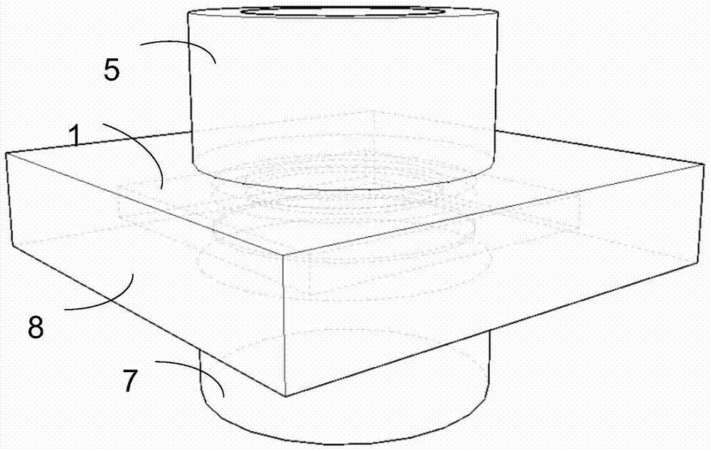
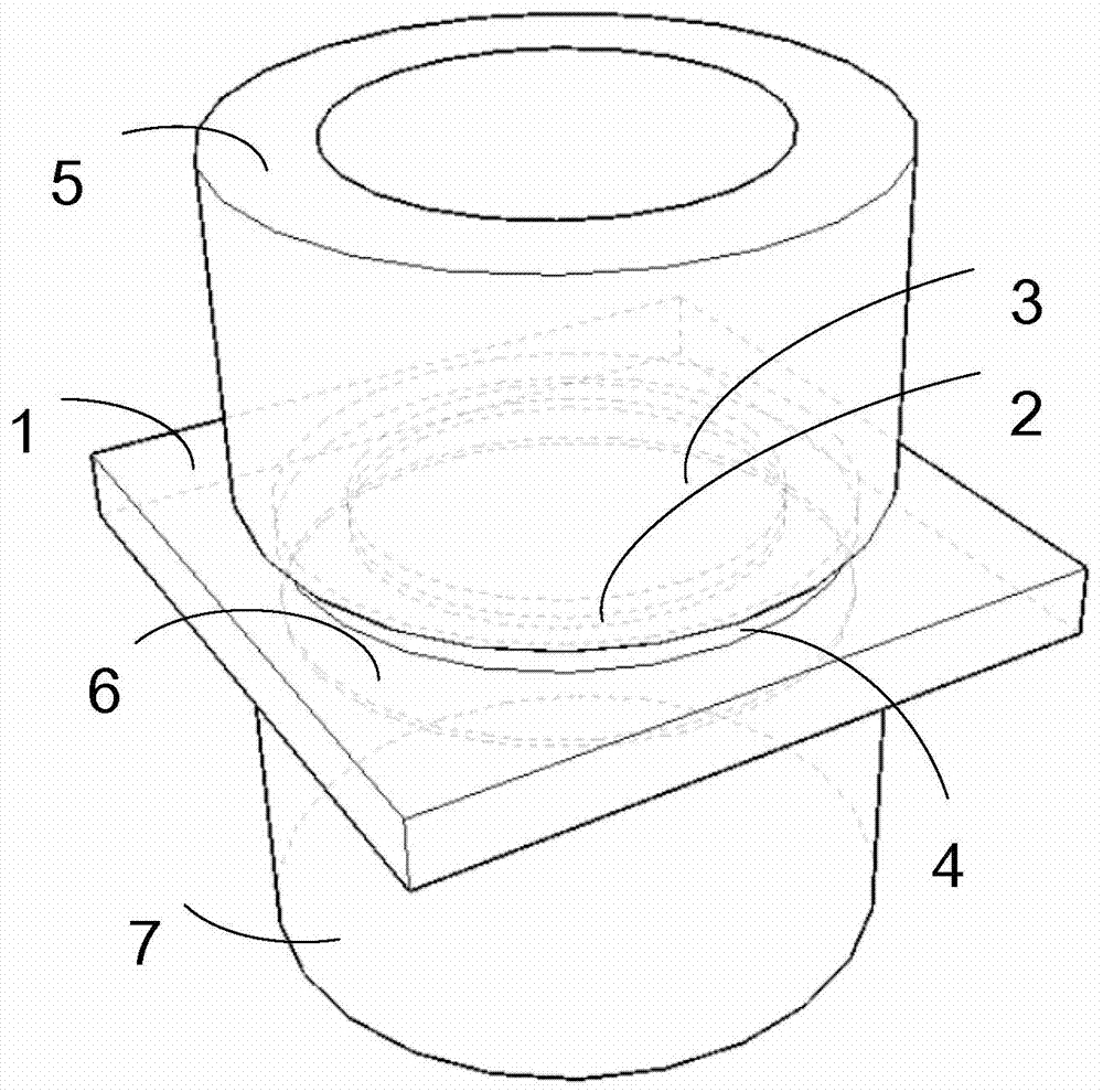
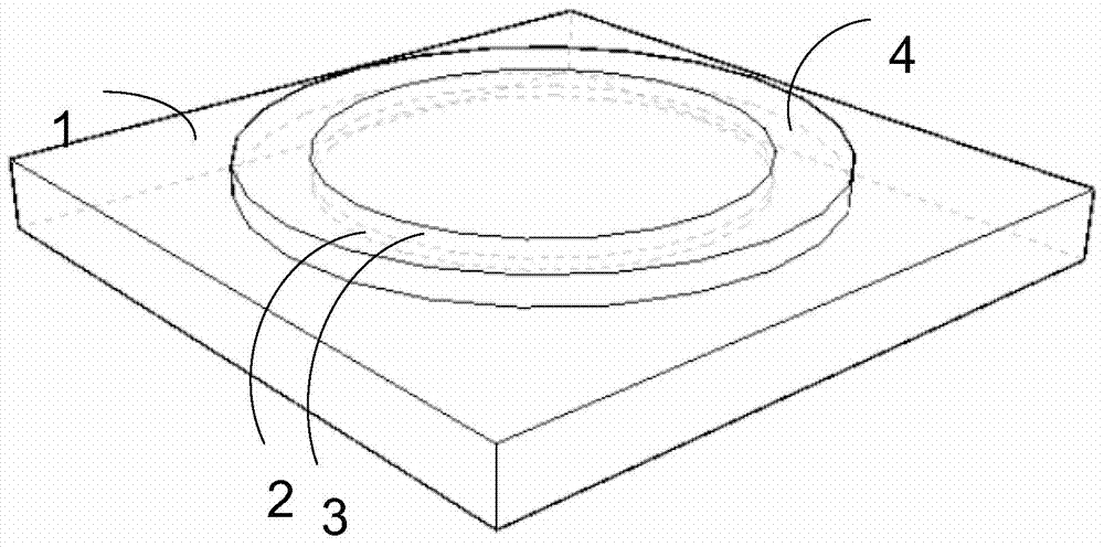
[0071] In this embodiment, a high-resistance 4H-SiC single crystal is used as the substrate material, and the crystal is cut into a 1mm thin slice along the (11-20) plane, and then cut into a 10mm X 10mm square high-resistance semiconductor 1, and six surfaces are polished to a roughness less than 0.2nm. After cleaning by the standard RCA process, etch at 1200°C for 0.5 hours in hydrogen with a pressure of 1 bar to eliminate the surface damage layer. Before use, immerse in 10% HF acid for 10 minutes, rinse with pure water for 30 minutes, use magnetron sputtering equipment to sputter metal Ni on one surface of the high-resistance semiconductor 1, and obtain a ring structure by photolithography (ie metal ring 4) and then annealed at 1100°C. Subsequently, the AlZnO transparent conductive layer 2 is deposited by magnetron sputtering equipment. Then adopt PECVD to deposit SiO2 anti-reflective passivation layer 3, such as image 3 shown. Deposit Ag on the other opposite surface ...

Embodiment 2

[0073] In this embodiment, a high-resistance 4H-SiC single crystal is used as the substrate material, and the crystal is cut into a 1mm thin slice along the (11-20) plane, and then cut into a disc-shaped high-resistance semiconductor 9 with a diameter of 10mm, and two large The face and sides are polished to a roughness of less than 0.2nm. After cleaning by the standard RCA process, etch at 1200°C for 0.5 hours in hydrogen with a pressure of 1 bar to eliminate the surface damage layer. Before use, immerse in HF acid with a concentration of 10% for 10 minutes, rinse with pure water for 30 minutes, use CVD equipment, heat at 1200°C under Ar atmosphere to form a graphene transparent conductive layer on the two facing large surfaces of SiC, Obtain circular graphene transparent conductive layer 10,11 by etching process, such as Figure 7 shown. Then, a magnetron sputtering device is used to sputter metal Ni on one surface of the high-resistance semiconductor 9, and a ring structu...


PUM


Abstract

The invention provides an opposite front light-in high-power photoconductive switch device and a making method thereof. The opposite front light-in high-power photoconductive switch device includes a hollow metal electrode, a metal ring, an antireflection passivation layer, a transparent conductive layer, a high-resistance semiconductor, a high-reflectivity electrode, and a solid metal electrode. The transparent conductive layer and the antireflection passivation layer are arranged in sequence on the high-resistance semiconductor used as a substrate, and the metal ring surrounding and connected around the transparent conductive layer and the antireflection passivation layer is also arranged on the high-resistance semiconductor. The side of the metal ring opposite to the substrate is connected with the hollow metal electrode. The high-reflectivity electrode is arranged on the back of the high-resistance semiconductor. The side of the high-reflectivity electrode opposite to the substrate is connected with the solid metal electrode. The device is packaged with a dielectric material with high breakdown field strength. Edge breakdown caused by uneven carriers can be avoided, and the withstand voltage and light efficiency of the switch can be greatly improved.

Description

technical field [0001] The invention belongs to the technical field of preparation of high-power semiconductor switching devices, and in particular relates to a high-power photoconductive switching device and a manufacturing method thereof. Background technique [0002] Switches are one of the essential components in power electronic circuits, and the properties of switches are particularly important in high-power systems. The so-called high-power system must withstand large voltage and current at the same time. The most direct problem that a large voltage brings to the device is the avalanche breakdown caused by the acceleration of the carrier by the strong electric field, and the thermal breakdown is easy to occur due to the thermal effect under the high current. These two failure modes are difficult problems faced by high-power switching devices. [0003] The high-power switch currently used in practical applications is a spark gap switch, which uses the discharge chann...

Claims


Application Information

Patent Timeline
Patent Type & Authority Applications(China)
IPC IPC(8): H01L31/02H01L31/0216H01L31/0224H01L31/0312H01L31/09H01L31/18
CPCH01L31/02002H01L31/0216H01L31/0224H01L31/0312H01L31/09H01L31/1812Y02P70/50
Inventor 黄维孔海宽施尔畏
Owner SHANGHAI INST OF CERAMIC CHEM & TECH CHINESE ACAD OF SCI
Why Eureka
Try Eureka