Method for cutting sapphire substrate LED chip through lasers

A sapphire substrate and LED chip technology, applied in laser welding equipment, electrical components, circuits, etc., can solve problems such as low cutting yield, poor appearance, and prone to double crystals, so as to improve cutting yield and improve appearance rate, to avoid the effect of twin crystals

Inactive Publication Date: 2018-01-05
SHANDONG INSPUR HUAGUANG OPTOELECTRONICS
View PDF10 Cites 17 Cited by
  • Summary
  • Abstract
  • Description
  • Claims
  • Application Information

AI Technical Summary

Problems solved by technology

The focus of the present invention is to solve the technical problem of poor appearance after cutting the sapphire substrate: the cutting depth of the chip surface layer with a thickness of sapphire substrate ≥ 150 μm cannot meet the requirements, and twin crystals, oblique cracks, and chipping will be formed; even if a single focus Stealth dicing, the dicing yield is still low, prone to twin crystals

Method used


Image

  • Method for cutting sapphire substrate LED chip through lasers
  • Method for cutting sapphire substrate LED chip through lasers
  • Method for cutting sapphire substrate LED chip through lasers

Examples


Embodiment 1

[0041] A method for cutting a sapphire substrate LED chip by laser, comprising:

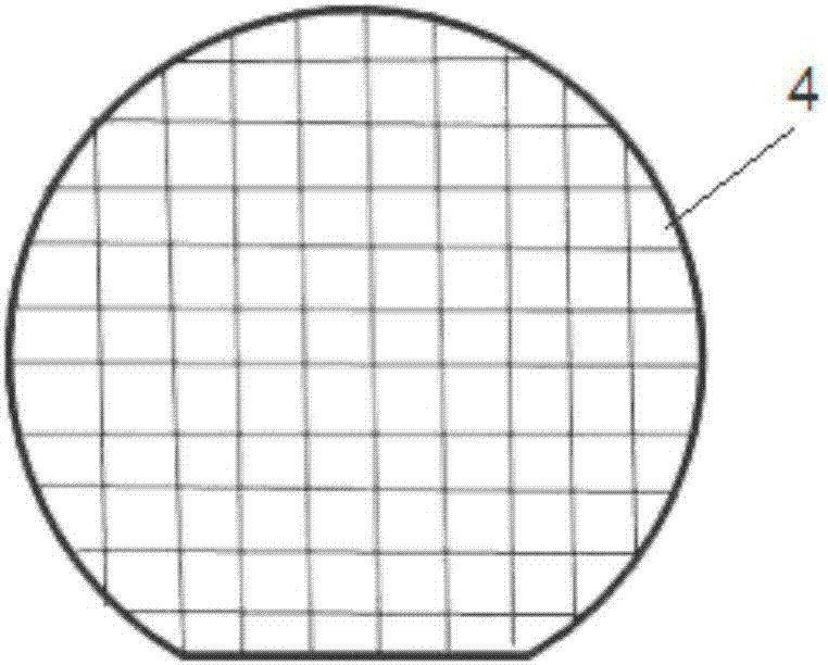
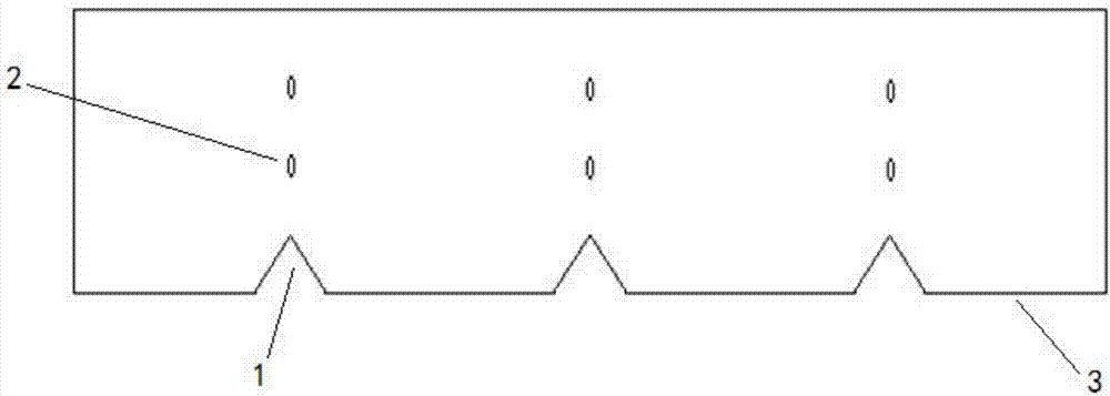
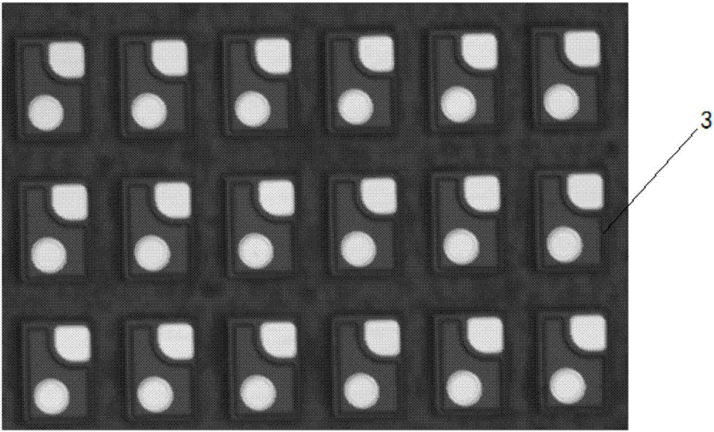
[0042] (1) Utilize the ultraviolet laser dicing machine to ablate and cut the groove 1 on the electrode surface 3 of the sapphire substrate wafer; the wafer refers to the LED chip that has completed the electrode but not cut; Refers to the thinned sapphire substrate wafer 4; the laser frequency in the Y direction of the wafer is 120-150KHz, the moving speed of the ultraviolet laser dicing machine is 110-130mm / s, and the laser frequency in the X direction of the wafer is 120-150KHz. It is 120-150KHz, and the moving speed of the ultraviolet laser scribing machine is 110-130mm / s;

[0043] (2) Invert the wafer so that the electrode surface is in contact with the white film, and the substrate is facing up, and placed on the platform of the invisible laser dicing machine, and the laser is applied to the sapphire substrate wafer by using the invisible laser dicing machine Inside: at least two parallel ...

Embodiment 2

[0048] A method for cutting a sapphire substrate LED chip by laser as described in Embodiment 1, the difference is that the thickness of the sapphire substrate wafer is 150-200 μm. When the thickness of the sapphire substrate wafer is 150-200 μm, it is sequentially cut out from the electrode surface: the first modified layer and the second modified layer, and the distance between the first modified layer and the electrode is The surface is 20-100 μm; the distance between the second modified layer and the first modified layer is 20-50 μm.

Embodiment 3

[0050] A kind of method utilizing laser cutting sapphire substrate LED chip as described in embodiment 1, its difference is, when the thickness of described sapphire substrate wafer is greater than or equal to 200 μm, at distance from described electrode surface (1 / 3) Cut ~(2 / 5) sapphire substrate wafer thickness position to form the first modified layer, and then prepare modified layers at intervals of 20-25 μm along the first modified layer to form parallel modified layer.


PUM

PropertyMeasurementUnit
thicknessaaaaaaaaaa
thicknessaaaaaaaaaa
depthaaaaaaaaaa

Abstract

According to a method for cutting a sapphire substrate LED chip through lasers, a paddle with the depth being 20-40 [mu]m is cut in the face, with an electrode, of a wafer through an ultraviolet laserwafer scriber; and modified layers are formed in the mode that an invisible laser wafer scriber is utilized to act on the interior of the wafer, that is, the different modified layers are formed in the mode that the lasers are focused on the positions, with different depths, of the wafer through adjustment of the laser focus depth of the invisible laser wafer scriber, and cracks generated throughstress releasing of the modified layers can be connected together. The sapphire substrate wafer machined through the method is cleaved in the direction of the cracks through a piece cleavage machine,so that the sapphire substrate wafer is cut into independent light emitting units, and thus, cutting is completed. According to the method for cutting the sapphire substrate LED chip through the lasers, the sapphire substrate wafer with the large thickness and size is cut, the cutting yield of the sapphire substrate wafer can be effectively increased, the cut chip is prevented from generating thephenomena of crystal twin, edge breakage and oblique cracking, and the appearance yield rate of the cut chip is effectively increased.

Description

technical field [0001] The invention relates to a method for cutting a sapphire substrate LED chip by using a laser, and belongs to the technical field of LED chip cutting. Background technique [0002] Sapphire substrate LED chips have been developed rapidly in recent years due to their advantages such as low energy consumption, high luminous efficiency, long life, green environmental protection, cold light source, fast response time, and can be used under various harsh conditions. A new generation of lighting sources. With the maturity of III-V semiconductor technology, the development of LED chips continues to develop in the direction of higher efficiency and higher brightness. As its application becomes more and more extensive, how to improve the luminous efficiency of GaN-based LEDs has increasingly become the focus of attention. The main factors affecting the luminous efficiency of LEDs are internal quantum efficiency and external quantum efficiency, and the improveme...

Claims


Application Information

Patent Timeline
Patent Type & Authority Applications(China)
IPC IPC(8): B23K26/364B23K26/53H01L33/00
Inventor 吴金凤李法健单立英赵霞焱肖成峰
Owner SHANDONG INSPUR HUAGUANG OPTOELECTRONICS
Why Eureka
Try Eureka