Epitaxial growth method of LED capable of improving luminous efficiency
A technology of epitaxial growth and luminous efficiency, which is applied in the direction of electrical components, circuits, semiconductor devices, etc., can solve the problems of luminous efficiency attenuation, etc., and achieve the effects of improving luminous efficiency, effective barrier height, and hole mobility
- Summary
- Abstract
- Description
- Claims
- Application Information
AI Technical Summary
Problems solved by technology
Method used
Image


Examples
Embodiment 1
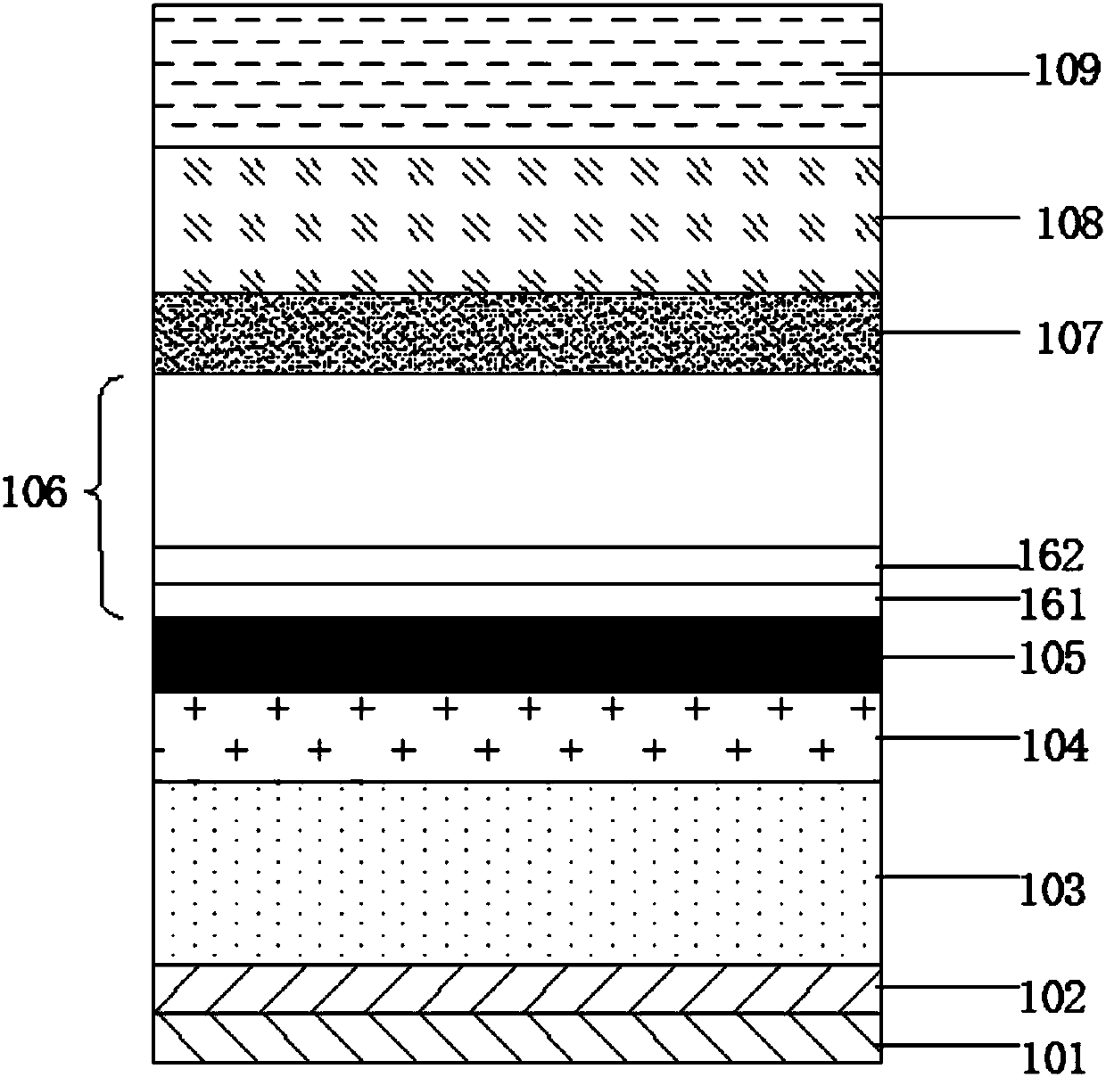
[0048] The LED epitaxial growth method for enhancing luminous radiation efficiency described in this embodiment includes the following steps:
[0049] Step 101, processing the sapphire substrate.
[0050] Step 102 , growing a low-temperature buffer layer GaN.
[0051] Step 103 , growing an undoped GaN layer.
[0052] Step 104 , growing a Si-doped N-type GaN layer.
[0053] Step 105, growing an InAlN:Mg thin barrier layer, further:
[0054] Keep the reaction chamber pressure at 400mbar-600mbar, keep the temperature at 800°C-900°C, and feed NH with a flow rate of 30000sccm-60000sccm 3 , TMAl of 100sccm-200sccm, N of 80L / min-110L / min 2 , 800sccm-1000sccm TMIn and 1200sccm-1500sccm CP 2 Mg, grow a Mg-doped InAlN layer with a thickness of 5nm-12nm to form an InAlN:Mg thin barrier layer, where the Mg doping concentration is 5E17atoms / cm 3 -8E17 atoms / cm 3 .(1E17 represents 10 to the 17th power, which is 10 17 , 5E17 represents 5×10 17 , atoms / cm 3 is the concentration unit...
Embodiment 2
[0065] This embodiment specifically describes the specific content of growing the LED epitaxial layer as a whole. The LED epitaxial growth method for improving luminous efficiency described in this embodiment includes the following steps:
[0066] Step 201, processing the sapphire substrate: into the reaction chamber of the metal-organic chemical vapor deposition system with the substrate placed, H at 1000°C-1100°C 2 Under the atmosphere, feed 100L / min-130L / min of H 2 , keep the reaction chamber pressure at 100mbar-300mbar, and process the sapphire substrate for 5min-10min.
[0067] Step 202, growing low-temperature buffer layer GaN: lower the temperature to 500°C-600°C, keep the reaction chamber pressure at 300mbar-600mbar, and feed NH with a flow rate of 10000sccm-20000sccm 3 , 50sccm-100sccm TMGa and 100L / min-130L / min H 2 , grow a low-temperature buffer layer GaN with a thickness of 20nm-40nm on a sapphire substrate.
[0068] Raise the temperature to 1000°C-1100°C, keep th...
Embodiment 3
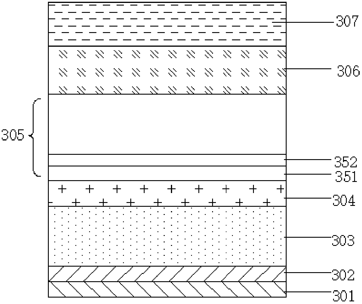
[0082] A conventional LED epitaxial growth method is provided below as a comparative example of the present invention.
[0083] A conventional LED epitaxial growth method includes the following steps:
[0084] Step 301, processing the sapphire substrate: Into the reaction chamber of the metal-organic chemical vapor deposition system with the substrate placed, H at 1000°C-1100°C 2 Under the atmosphere, feed 100L / min-130L / min of H 2 , keep the reaction chamber pressure at 100mbar-300mbar, and process the sapphire substrate for 5min-10min.
[0085] Step 302, grow low-temperature buffer layer GaN: lower the temperature to 500°C-600°C, keep the reaction chamber pressure at 300mbar-600mbar, and feed NH with a flow rate of 10000sccm-20000sccm 3 , 50sccm-100sccm TMGa and 100L / min-130L / min H 2 , grow a low-temperature buffer layer GaN with a thickness of 20nm-40nm on a sapphire substrate.
[0086] Raise the temperature to 1000°C-1100°C, keep the reaction chamber pressure at 300mbar...
PUM
 Abstract
Description
Claims
Application Information
 - R&D
- Intellectual Property
- Life Sciences
- Materials
- Tech Scout
- Unparalleled Data Quality
- Higher Quality Content
- 60% Fewer Hallucinations
Browse by: Latest US Patents, China's latest patents, Technical Efficacy Thesaurus, Application Domain, Technology Topic, Popular Technical Reports.
© 2025 PatSnap. All rights reserved.Legal|Privacy policy|Modern Slavery Act Transparency Statement|Sitemap|About US| Contact US: help@patsnap.com