Nickel oxide thin film and its preparation method, functional material, thin film structure manufacturing method and electroluminescent device

A technology of electroluminescent devices and thin film structures, applied in the direction of electric solid devices, nickel oxide/nickel hydroxide, electrical components, etc., can solve the problem that the surface work function of nickel oxide conductive thin films cannot meet the requirements of OLED devices and QLED devices, etc. Achieve the effect of improving hole injection rate, improving performance and stability

Active Publication Date: 2021-02-26
ZHEJIANG UNIV +1
View PDF1 Cites 0 Cited by
  • Summary
  • Abstract
  • Description
  • Claims
  • Application Information

AI Technical Summary

Problems solved by technology

[0006] The main purpose of the present invention is to provide a kind of nickel oxide thin film and preparation method thereof, functional material, the preparation method of thin film structure and electroluminescence device, to solve the surface work function of nickel oxide conductive thin film in the prior art can not satisfy OLED device and Questions about QLED device requirements

Method used


Image

  • Nickel oxide thin film and its preparation method, functional material, thin film structure manufacturing method and electroluminescent device
  • Nickel oxide thin film and its preparation method, functional material, thin film structure manufacturing method and electroluminescent device
  • Nickel oxide thin film and its preparation method, functional material, thin film structure manufacturing method and electroluminescent device

Examples


preparation example Construction

[0037] In yet another typical embodiment of the present application, a method for preparing the above-mentioned nickel oxide film is provided, the preparation method comprising: placing a nickel oxide precursor solution on a carrier, performing the first annealing, and forming nickel oxide film layer; after the nickel oxide film layer is treated with ultraviolet-ozone, organic molecules are arranged on the surface of the nickel oxide film layer; and the nickel oxide film layer provided with organic molecules is annealed for the second time in nitrogen or inert gas atmosphere, Nickel oxide thin film

[0038] The nickel oxide precursor solution is annealed for the first time to obtain a nickel oxide film; then, through the ultraviolet-ozone treatment of the nickel oxide film, on the one hand, a layer of hydroxyl radicals is generated on the surface of the nickel oxide to provide On the other hand, clean the nickel oxide film layer to improve the binding force of organic molecule...

Embodiment 1

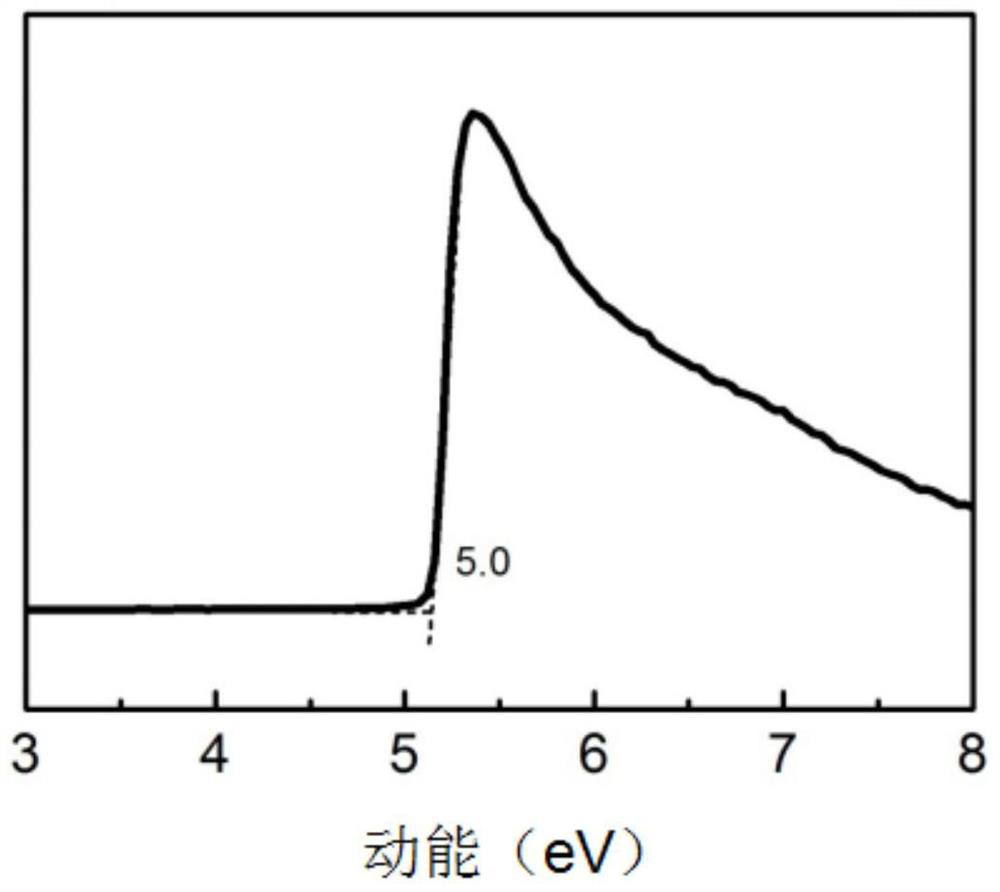
[0054] S1: Nickel nitrate and glycine were dissolved in water at a molar ratio of 3:5 to prepare a nickel oxide precursor solution, in which the concentration of nickel nitrate was 0.06 mol / L. The nickel oxide precursor was coated on the ITO substrate by spin coating (rotational speed: 4000rpm), and the nickel oxide precursor solution was annealed in air at 200° C. for 60 min to obtain a nickel oxide film.

[0055] S2: Treat the nickel oxide film layer with ultraviolet-ozone for 20 minutes, and the irradiation power of the ultraviolet lamp is 200W. 2 In an atmospheric glove box, a trifluoromethylbenzoic acid / ethanol solution with a concentration of 3mmol / L was spin-coated on the ITO / nickel oxide composite film (rotating speed: 2000rpm).

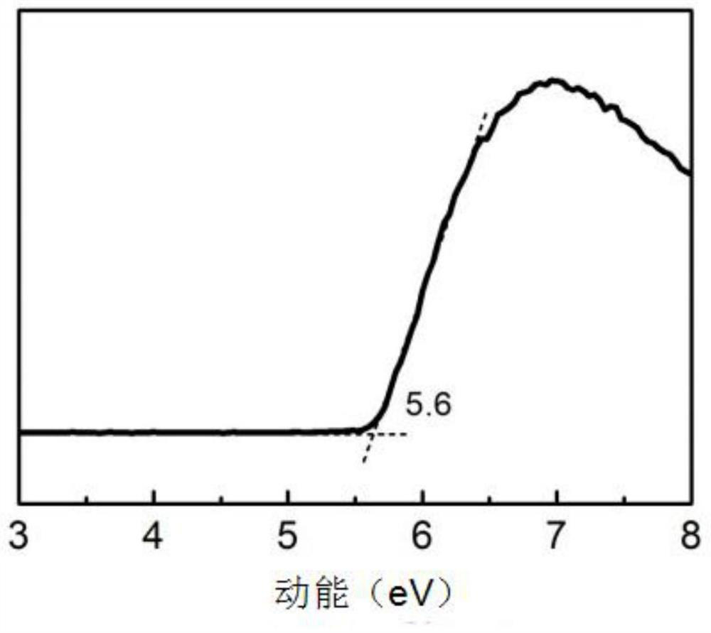
[0056] S3: In the glove box, place the above film on a heating panel, anneal at 120°C for 30 minutes, then wash the surface three times with ethanol, and dry to obtain a nickel oxide film, that is, a surface-modified ITO / nickel oxide composit...

Embodiment 2

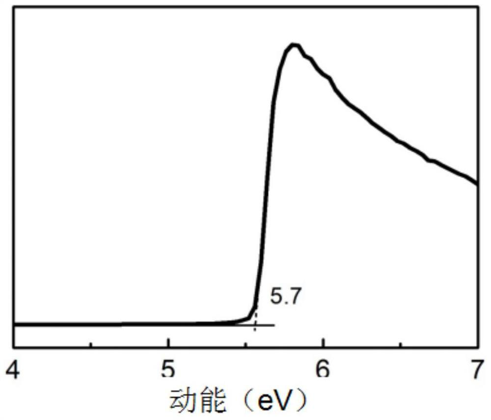
[0058] The specific steps, materials and instruments used are the same as those in Example 1, except that the annealing temperature in step S3 is 140°C. The thin film is tested by ultraviolet photoelectric spectroscopy, and the test results are shown in image 3 , In this embodiment, the surface work function of ITO / nickel oxide is 5.7eV.


PUM

PropertyMeasurementUnit
electron work functionaaaaaaaaaa

Abstract

The invention provides a nickel oxide thin film and its preparation method, functional material, thin film structure manufacturing method and electroluminescent device. The nickel oxide film comprises: a nickel oxide film layer; organic molecules with electron-withdrawing groups, and the organic molecules are connected and arranged on the surface of the nickel oxide film layer. The organic molecule uses the electron-withdrawing group to form a chemical bond with the hydroxyl radical on the surface of the nickel oxide film to form a stable connection, and due to the existence of the organic molecule with the electron-withdrawing group, it is equivalent to establishing a reverse nickel oxide on the surface of the nickel oxide. The electric field increases the surface work function of the nickel oxide film. Furthermore, when the nickel oxide thin film with high surface work function of the present application is applied to QLED devices and OLED devices, the hole injection rate is improved, and the use of PEDOT:PSS which is harmful to the device can be avoided, thereby improving the performance and stability of the device sex.

Description

technical field [0001] The invention relates to the field of optoelectronic devices, in particular to a nickel oxide thin film, a preparation method thereof, a functional material, a method for manufacturing a thin film structure, and an electroluminescent device. Background technique [0002] Indium tin oxide (Indium tin oxide, referred to as ITO) transparent conductive film has excellent electrical conductivity, and has >90% light transmittance, widely used as organic electroluminescent device (Organic Light-Emitting Diode, referred to as OLED), quantum It is used as electrodes of optoelectronic devices such as Quantum Dot Light-Emitting Diode (QLED for short), Organic Photovoltaic (OPV for short), and also serves as a light-transmitting window at the same time. [0003] At present, the surface work function of conventional ITO is 4.5eV-4.8eV, which is lower than the highest electron-occupied orbital (Highest Occupied Molecular Orbital, HOMO) of most organic functional ...

Claims


Application Information

Patent Timeline
Patent Type & Authority Patents(China)
IPC IPC(8): H01L51/50H01L51/56
CPCH10K85/111H10K85/115H10K50/17H10K2102/00H10K71/10H10K85/633H10K85/631H10K71/00C01G53/04C01P2006/40H10K71/40H10K71/135H10K2102/361
Inventor 金一政梁骁勇陈超
Owner ZHEJIANG UNIV
Why Eureka
Try Eureka