Three-dimensional through silicon via vertical interconnection method based on multi-layer graphene auxiliary layer

A multi-layer graphene and auxiliary layer technology, which is applied in the manufacturing of electrical components, electrical solid-state devices, semiconductor/solid-state devices, etc. performance and reliability, improving the effect of signal fidelity transmission

Inactive Publication Date: 2018-02-02
XUZHOU NORMAL UNIVERSITY
View PDF6 Cites 4 Cited by
  • Summary
  • Abstract
  • Description
  • Claims
  • Application Information

AI Technical Summary

Problems solved by technology

[0004] In view of the problems existing in the above-mentioned prior art, the present invention provides a three-dimensional through-silicon via vertical interconnection method based on a multilayer graphene auxi...

Method used


Image

  • Three-dimensional through silicon via vertical interconnection method based on multi-layer graphene auxiliary layer
  • Three-dimensional through silicon via vertical interconnection method based on multi-layer graphene auxiliary layer
  • Three-dimensional through silicon via vertical interconnection method based on multi-layer graphene auxiliary layer

Examples


Embodiment

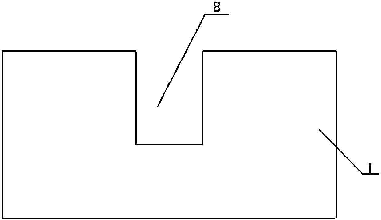
[0039] Such as figure 1 As shown, the silicon hole 8 is made on the silicon substrate 1 by deep reactive ion etching, laser etching or wet etching; the diameter of the silicon hole 8 is 1 micron to 100 microns, and the cross section of the silicon hole 8 is generally The silicon hole 8 is circular, and the aspect ratio of the silicon hole 8 is generally 1-30.

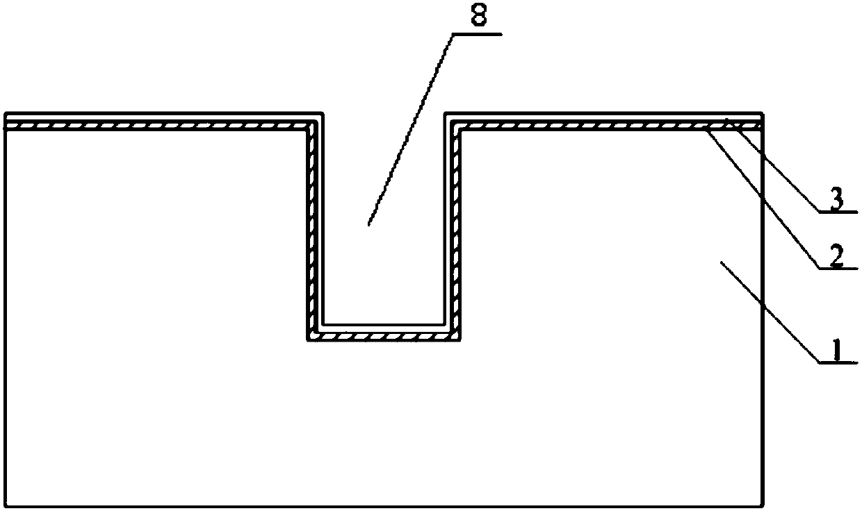
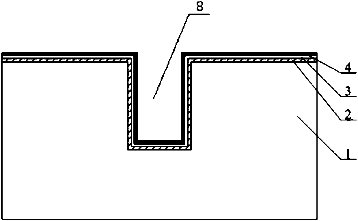
[0040] Such as figure 2 As shown, an insulating layer 2 is deposited on the surface of the silicon substrate 1 and the inner wall (circumferential surface and bottom surface) of the silicon hole 8. The deposition of the insulating layer 2 is made by thermal oxidation, chemical vapor deposition or physical vapor deposition. The material of the insulating layer 2 Silicon dioxide, alumina, etc., polyimide, parylene, etc. can be used, and the thickness of the insulating layer 2 is 0.5 to 1 micron; a barrier layer 3 is deposited on the insulating layer 2, and the barrier layer 3 is magnetron sputtered , physical vapor dep...


PUM


Abstract

The invention discloses a three-dimensional through silicon via vertical interconnection method based on a multi-layer graphene auxiliary layer, which comprises the steps of manufacturing a silicon via in a silicon substrate; depositing an insulating layer at the surface of the silicon substrate and the inner wall of the silicon via; depositing a barrier layer on the insulating layer; forming a multi-layer graphene auxiliary layer at the surface of the barrier layer; attaching a dry film to the multi-layer graphene auxiliary layer at the surface of the silicon substrate, and then performing exposure and development to form a dry film layer; depositing a seed layer at the bottom surface of the silicon via and the surface of the dry film layer; and filling the silicon via with a conductive material. According to the invention, a via is manufactured in the silicon substrate, then an insulating layer and a barrier layer are successively deposited, a multi-layer graphene auxiliary layer isformed, a dry film is attached, a seed layer is deposited, and then the via is filled with a conductive material, excellent electrical performance of the graphene material is utilized to solve a problem of increase in resistance and power consumption of the TSV (Through Silicon Via) caused by a skin effect, atom migration and the like, the graphene and copper serve as a TSV signal transmission channel, the electrical performance and the reliability of the 3D-TSV structure are improved, and problems such as TSV vertical interconnection and signal fidelity under a new technology node are improved.

Description

technical field [0001] The invention relates to a method for vertical interconnection of through-silicon holes, in particular to a method for vertical interconnection of three-dimensional through-silicon holes based on a multilayer graphene auxiliary layer, and belongs to the technical field of microelectronic packaging. Background technique [0002] With the continuous improvement of integrated circuit (IC, Integrated Circuit) chip performance requirements, such as function enhancement, size reduction, energy consumption and cost reduction, etc., microelectronic packaging technology is facing new challenges. In order to meet the requirements of IC products, three-dimensional packaging technology came into being. It makes full use of the z-direction space, greatly reduces the interconnection length, improves packaging density, reduces power consumption, and has a higher chip function integration. Through silicon via vertical interconnection (TSV, Through Silicon Via) techno...

Claims


Application Information

Patent Timeline
IPC IPC(8): H01L21/768H01L23/48
CPCH01L21/76898H01L23/481
Inventor 陆向宁宿磊何贞志樊梦莹刘凡
Owner XUZHOU NORMAL UNIVERSITY
Why Eureka
Try Eureka