Normally-closed GaN-based MOSFET structure with high threshold voltage and high conduction performance and fabrication method thereof

A high-threshold voltage, high conduction technology, applied in semiconductor/solid-state device manufacturing, circuits, electrical components, etc., can solve problems such as the inability to achieve precise and controllable thin barrier layer thickness, small device threshold voltage, and high interface state density , to achieve the effects of reducing the concentration of two-dimensional electron gas, increasing the threshold voltage, and low on-resistance

Pending Publication Date: 2018-03-06
SUN YAT SEN UNIV
View PDF4 Cites 6 Cited by
  • Summary
  • Abstract
  • Description
  • Claims
  • Application Information

AI Technical Summary

Problems solved by technology

Completely removing the AlGaN layer in the gate area can increase the threshold voltage of the device, but it also brings problems such as low gate mobility, large on-resistance, and high interface state density.
Thinning the AlGaN layer in the gate region can alleviate this problem. However, due to the existence of the thin layer of AlGaN, there is a certain concentration of two-dimensional electron gas in the gate region, which makes the threshold voltage of the device smaller.
In addition, traditional thin barrier layer devices use methods such as etching to remove the AlGaN layer in the gate region. This method cannot achieve precise controllability of the thickness of the thin barrier layer, and will inevitably introduce lattice damage in the gate region.

Method used


Image

  • Normally-closed GaN-based MOSFET structure with high threshold voltage and high conduction performance and fabrication method thereof
  • Normally-closed GaN-based MOSFET structure with high threshold voltage and high conduction performance and fabrication method thereof
  • Normally-closed GaN-based MOSFET structure with high threshold voltage and high conduction performance and fabrication method thereof

Examples


Embodiment 1

[0039] like Figure 11 Shown is a schematic diagram of the device structure of this embodiment, and its structure includes a substrate 1, a stress buffer layer 2, a GaN epitaxial layer 3, an AlN epitaxial layer 4, an AlGaN epitaxial layer 5, a secondary epitaxial layer 6, and a second epitaxial layer from bottom to top. A groove is formed by sub-epitaxy, a gate dielectric layer 7, a source 8 and a drain 9 are formed at both ends, and a gate 10 is covered on the dielectric layer 7 at the channel of the groove.

[0040] The preparation method of the above-mentioned normally-off GaN-based MOSFET with high threshold voltage and high conduction performance is as follows: Figure 1-Figure 11 shown, including the following steps:

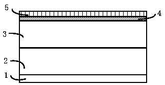
[0041] S1, utilize metal-organic chemical vapor deposition method to grow a layer of stress buffer layer 2 on Si substrate 1, such as figure 1 shown;

[0042] S2. Using a metal organic chemical vapor deposition method to grow a GaN epitaxial layer 3 on t...

Embodiment 2

[0055] like Figure 13 Shown is a schematic diagram of the device structure of this embodiment, which differs from the structure of Embodiment 1 only in that in Embodiment 1, the AlN layer 4 and the AlGaN layer 5 above the gate region are retained by selective etching by photolithography, while In the embodiment 2, the AlN layer 4 and the AlGaN layer 5 are not etched, and the AlN layer 4 and the AlGaN layer 5 remain. On this substrate, a secondary epitaxial AlGaN layer 6 is grown in a selected region to form a recessed gate.


PUM


Abstract

The invention relates to the technical field of semiconductor, in particular to a normally-closed GaN-based MOSFET structure with a high threshold voltage and high conduction performance and a fabrication method thereof. The fabrication method of the normally-closed GaN-based MOSFET structure with the high threshold voltage and high conduction performance comprises the following steps of firstly,providing a required substrate, sequentially and epitaxially growing a stress buffer layer, a GaN buffer layer, an AIN thin layer and an AlGaN thin layer on the substrate, and reserving the AlN thin layer and the AlGaN thin layer on a grid region by etching to obtain a substrate for epitaxy of a selection region; secondly, sequentially selecting a regional epitaxial GaN channel layer, a AIN insertion layer and a AIGaN barrier layer on the substrate to form a groove structure; and finally, depositing a grid dielectric layer, covering grid metal on a groove channel grid dielectric layer, and covering two ends of the grid with metal to form a source and a drain. By the fabrication method, the threshold voltage and the grid region mobility can be effectively improved, the channel resistance isreduced, and the conduction performance of the GaN MOSFET device is improved.

Description

technical field [0001] The invention relates to the technical field of semiconductors, and more specifically, to a normally-off GaN-based MOSFET structure with high threshold voltage and high conduction performance and a preparation method thereof. Background technique [0002] As a representative of the third-generation wide-bandgap semiconductor materials, GaN materials have superior properties such as large bandgap width, high breakdown electric field strength, large saturated electron drift velocity, and high thermal conductivity. GaN-based power switching devices usually use two-dimensional electron gas with high concentration and high mobility at the interface of AlGaN / GaN heterostructure to work, so that the device has the advantages of small on-resistance and fast switching speed, and is very suitable for making high-power, high-frequency , High temperature power electronic devices. [0003] In the field of power electronics applications, in order to ensure the fail...

Claims


Application Information

Patent Timeline
Patent Type & Authority Applications(China)
IPC IPC(8): H01L21/336H01L29/06H01L29/78
CPCH01L29/0684H01L29/66522H01L29/66621H01L29/78
Inventor 刘扬张佳琳
Owner SUN YAT SEN UNIV
Why Eureka
Try Eureka