Semiconductor device and manufacturing method thereof

A semiconductor and device technology, applied in the field of semiconductor devices and their preparation, can solve problems such as uneven thickness, affecting the performance of resistance devices, and poor uniformity of resistance device characteristics

Active Publication Date: 2020-07-31
CSMC TECH FAB2 CO LTD
View PDF3 Cites 0 Cited by
  • Summary
  • Abstract
  • Description
  • Claims
  • Application Information

AI Technical Summary

Problems solved by technology

But now it is found that the thickness of the dielectric layer is often uneven, resulting in poor uniformity of the characteristics of the resistance device, which affects the performance of the resistance device

Method used


Image

  • Semiconductor device and manufacturing method thereof
  • Semiconductor device and manufacturing method thereof
  • Semiconductor device and manufacturing method thereof

Examples


Embodiment 1

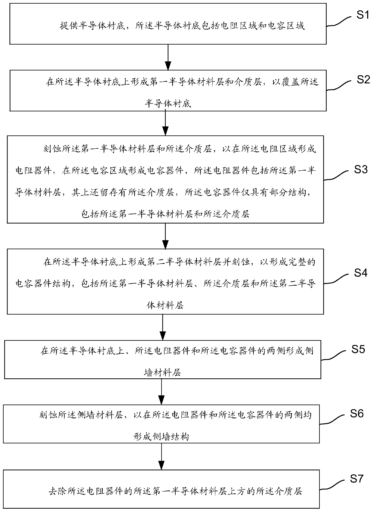
[0043] In order to solve the problems existing in the prior art, the present invention provides a method for preparing a semiconductor device. The structure will be further described below in conjunction with the accompanying drawings, wherein figure 1 Shows a flow chart of the fabrication process of the semiconductor device of the present invention; figure 2A cross-sectional view showing a structure formed in relevant steps of a method for manufacturing a semiconductor device in an embodiment of the present invention; image 3 A cross-sectional view showing a structure formed in relevant steps of a method for manufacturing a semiconductor device in an embodiment of the present invention; Figure 4 A cross-sectional view showing a structure formed in relevant steps of a method for manufacturing a semiconductor device in an embodiment of the present invention; Figure 5 A cross-sectional view showing a structure formed in relevant steps of a method for manufacturing a semicon...

Embodiment 2

[0097] First, step 1 is performed to provide a semiconductor substrate, where the semiconductor substrate includes a resistance region and a capacitance region.

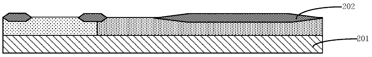
[0098] Specifically, such as figure 2 As shown, a semiconductor substrate 201 is provided, which at least includes a resistive region and a capacitive region.

[0099] Specifically, the semiconductor substrate may be at least one of the materials mentioned below: silicon, silicon-on-insulator (SOI), silicon-on-insulator (SSOI), silicon-germanium-on-insulator (S-SiGeOI) , silicon germanium on insulator (SiGeOI) and germanium on insulator (GeOI), etc.

[0100] N-wells and P-wells are formed in the semiconductor substrate, and the methods for forming the N-wells and P-wells can refer to methods commonly used in the art, and are not limited to a certain one, which will not be repeated here.

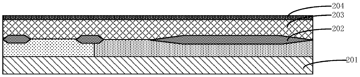
[0101] Optionally, after forming the N well and the P well, a field oxygen layer 202 is formed on the surface of the semiconduc...

Embodiment 3

[0141] The present invention also provides a semiconductor device, the semiconductor device comprising:

[0142] a semiconductor substrate comprising a resistive region and a capacitive region;

[0143] a resistive device formed in the resistive region, the resistive device comprising the first layer of semiconductor material;

[0144] a capacitive device structure formed in the capacitive region, the capacitive device structure including the first semiconductor material layer, the dielectric layer and the second semiconductor material layer;

[0145] Wherein the dielectric layer above the first semiconductor material layer of the resistance device has been removed.

[0146] Optionally, sidewall structures are formed on sidewalls of the resistive device and the capacitive device structure.

[0147] Wherein, the semiconductor substrate may be at least one of the materials mentioned below: silicon, silicon-on-insulator (SOI), silicon-on-insulator (SSOI), silicon-germanium-on-i...


PUM


Abstract

The invention provides a semiconductor device and a manufacturing method thereof. The method comprises the steps of providing a semiconductor substrate comprising a resistive region and a capacitive region; forming a first semiconductor material layer and a dielectric layer on the semiconductor substrate; etching the first semiconductor material layer and the dielectric layer to form a resistive device and a capacitive device, the capacitive device having only a partial structure comprising the first semiconductor material layer and the dielectric layer; forming a second semiconductor materiallayer on the semiconductor substrate and etching the second semiconductor material layer to form a complete capacitive device structure comprising the first semiconductor material layer, the dielectric layer and the second semiconductor material layer; forming a sidewall material layer on two sides of the semiconductor substrate, the resistive device and the capacitive device; etching the sidewall material layer to form sidewall structures on the two sides of the resistive device and the capacitive device; and removing the dielectric layer on the first semiconductor material layer of the resistive device.

Description

technical field [0001] The invention relates to the field of semiconductors, in particular, the invention relates to a semiconductor device and a preparation method thereof. Background technique [0002] At present, various semiconductor devices, such as transistors, resistors, and capacitors, are often used in integrated circuits at the same time. In order to improve production efficiency, when manufacturing integrated circuits, various semiconductor devices are often made to share the same manufacturing process as much as possible. For example, a resistive device generally has a polycrystalline layer structure, while a capacitive device generally has a dielectric structure sandwiched between two polycrystalline layers. made in steps. However, in the actual manufacturing process, the first polycrystalline layer and the intermediate dielectric layer are deposited at the same time, and then etched to form part of the structure of the resistive device and the capacitive devi...

Claims


Application Information

Patent Timeline
Patent Type & Authority Patents(China)
IPC IPC(8): H01L21/822H01L23/64
CPCH01L21/822H01L23/642H01L23/647H01L28/20H01L28/40
Inventor 陈雪磊李晓明杨俊
Owner CSMC TECH FAB2 CO LTD
Why Eureka
Try Eureka