Back channel etched oxide semiconductor tft substrate and method of making the same

A technology of oxide semiconductors and production methods, which is applied in the manufacture of semiconductor/solid-state devices, semiconductor devices, transistors, etc., can solve the problems of complex preparation process of IGZOTFT, low reliability of TFT devices, and easy damage to the channel region, so as to save The effect of etching barrier mask, low production cost, and small number of film defects

Active Publication Date: 2020-04-28
SHENZHEN CHINA STAR OPTOELECTRONICS SEMICON DISPLAY TECH CO LTD
View PDF5 Cites 0 Cited by
  • Summary
  • Abstract
  • Description
  • Claims
  • Application Information

AI Technical Summary

Problems solved by technology

However, the preparation process of IGZO TFT with ESL structure is relatively complicated, and it needs to go through six yellow light processes, which is not conducive to reducing costs. Therefore, the industry generally pursues the development of IGZO TFT with back channel etching (BCE) structure with fewer yellow light processes.
[0012] Since the IGZO TFT of the BCE structure is not provided with an etching barrier layer to block the back channel, the channel region of the IGZO active layer is easily damaged during the etching process of the source and drain electrodes, and due to the number of film defects in the IGZO active layer More, so IGZO TFT is sensitive to the environment, light, water vapor (H 2 O), oxygen (O 2 ), hydrogen (H 2 ) and organics (Organics) are likely to affect the performance of the TFT, resulting in lower reliability of the TFT device and a shorter service life of the panel

Method used


Image

  • Back channel etched oxide semiconductor tft substrate and method of making the same
  • Back channel etched oxide semiconductor tft substrate and method of making the same
  • Back channel etched oxide semiconductor tft substrate and method of making the same

Examples


Embodiment Construction

[0040] In order to further illustrate the technical means adopted by the present invention and its effects, the following describes in detail in conjunction with preferred embodiments of the present invention and accompanying drawings.

[0041] see figure 1 , the present invention provides a method for fabricating a back channel etched oxide semiconductor TFT substrate, comprising the following steps:

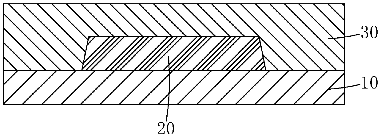
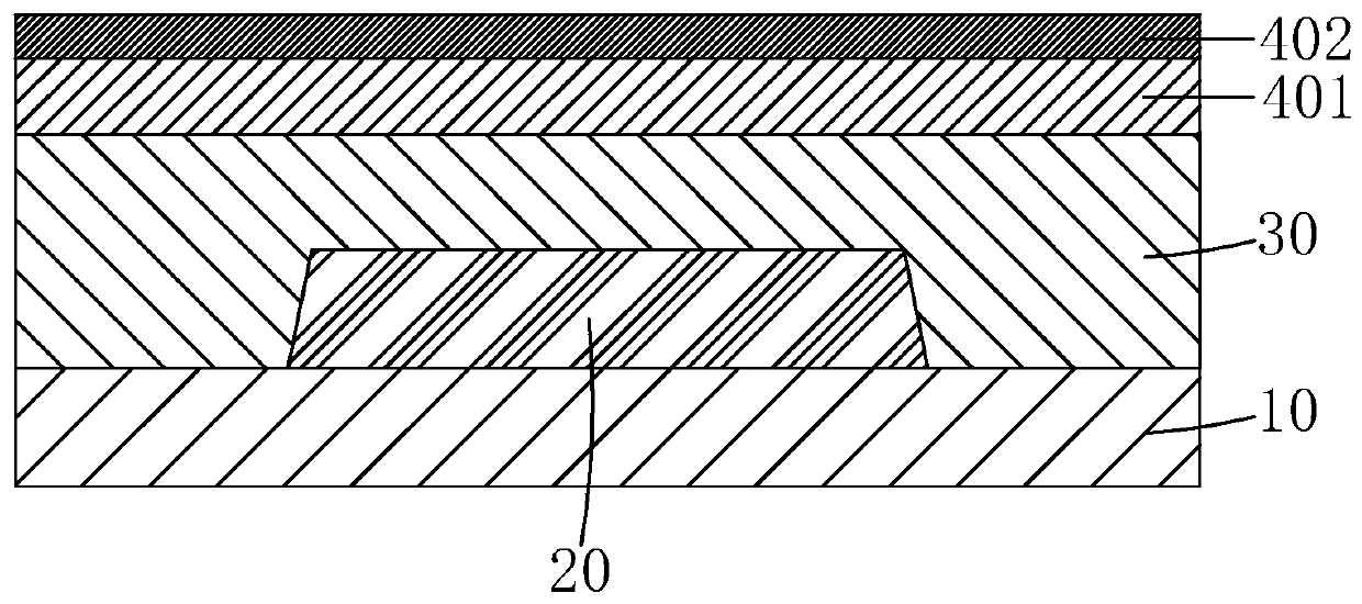
[0042] Step 1, such as figure 2 As shown, a base substrate 10 is provided, a metal material is deposited on the base substrate 10 and etched to form a gate 20 , and a gate insulating layer 30 covering the gate 20 is formed on the base substrate 10 .

[0043] Specifically, the base substrate 10 is a glass substrate.

[0044] Specifically, the step 1 further includes: cleaning and baking the base substrate 10 before forming the gate 20 on the base substrate 10 .

[0045] Specifically, the material of the gate 20 includes one or more of molybdenum (Mo), aluminum (Al), and copp...


PUM

PropertyMeasurementUnit
densityaaaaaaaaaa
densityaaaaaaaaaa

Abstract

The invention provides a back channel etching type oxide semiconductor TFT substrate and a manufacturing method thereof. In the manufacturing method of the back channel etching type oxide semiconductor TFT substrate of the present invention, the active layer is set as a double-layer structure, the first oxide semiconductor layer located in the lower layer is prepared according to normal deposition process parameters, and has a normal density, and the first oxide semiconductor layer located in the upper layer is prepared according to normal deposition process parameters and has a normal density. The dioxide semiconductor layer is prepared by changing the deposition process parameters and has a higher density; the first oxide semiconductor layer has a lower density and has a higher mobility, and the second oxide semiconductor layer has a higher density, The thin film has few defects and strong etching resistance, which can reduce the damage to the channel region of the active layer during the etching process of the drain and source electrodes, saves the mask of the etching barrier layer at the same time, and has low production cost.

Description

technical field [0001] The invention relates to the field of display technology, in particular to a back channel etching type oxide semiconductor TFT substrate and a manufacturing method thereof. Background technique [0002] Liquid crystal display (Liquid Crystal Display, LCD) has many advantages such as thin body, power saving, no radiation, etc., and has been widely used, such as: mobile phone, personal digital assistant (PDA), digital camera, computer screen or notebook computer screen etc. [0003] Organic light-emitting diode (Organic Light-Emitting Diode, OLED) display, also known as organic electroluminescent display, is a new type of flat panel display device, due to its simple preparation process, low cost, low power consumption, high luminance, Wide range of working temperature, light and thin size, fast response speed, easy to realize color display and large-screen display, easy to realize matching with integrated circuit driver, easy to realize flexible display...

Claims


Application Information

Patent Timeline
Patent Type & Authority Patents(China)
IPC IPC(8): H01L27/12H01L27/32H01L51/56
CPCH01L27/127H10K59/125H10K71/00H01L29/66969H01L29/7869H01L29/78696H01L21/44H01L21/47635H01L27/1225
Inventor 余明爵徐源竣周星宇
Owner SHENZHEN CHINA STAR OPTOELECTRONICS SEMICON DISPLAY TECH CO LTD
Why Eureka
Try Eureka