
A micro-energy harvester based on piezoelectric thick film mems technology and its preparation method

A micro-energy, harvester technology, used in the manufacture/assembly of piezoelectric/electrostrictive devices, piezoelectric/electrostrictive/magnetostrictive devices, piezoelectric effect/electrostrictive or magnetostrictive motors, etc. It can solve the problems of poor piezoelectric performance and simple design structure of piezoelectric films, and achieve the effects of diverse and complex device structures, high preparation efficiency and strong controllability.

Active Publication Date: 2020-06-12
SUZHOU UNIV
View PDF5 Cites 1 Cited by
  • Summary
  • Abstract
  • Description
  • Claims
  • Application Information

AI Technical Summary

Problems solved by technology

[0007] Aiming at the deficiencies of the prior art, the present invention provides a micro-energy harvester based on piezoelectric thick-film MEMS technology and its preparation method, which has greatly improved piezoelectric performance of piezoelectric thick-film, and can prepare device structures of diversification and The advantages of higher complexity solve the problem of poor piezoelectric performance and simple design structure of the piezoelectric film prepared by the traditional process

Method used


Image

  • A micro-energy harvester based on piezoelectric thick film mems technology and its preparation method
  • A micro-energy harvester based on piezoelectric thick film mems technology and its preparation method

Examples


Embodiment 1

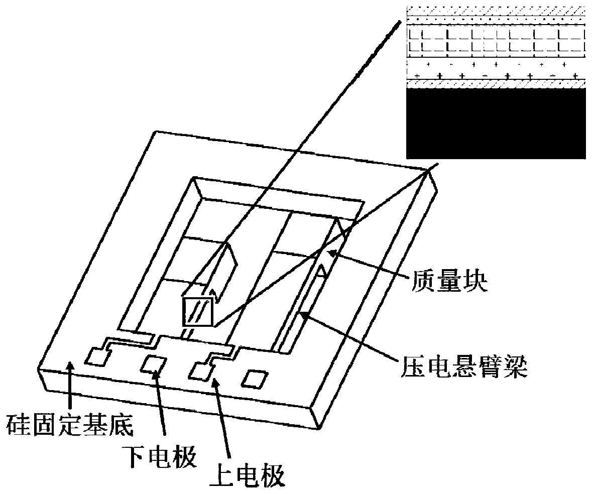
[0038] figure 1 It is a three-dimensional structure diagram of a micro-energy harvester, including: an upper electrode, a lower electrode, a silicon fixed base, a piezoelectric cantilever beam, and a quality block fixedly connected to one end of the piezoelectric cantilever beam and suspended in the air. Wherein, one end of the piezoelectric cantilever beam is fixedly connected to the inner side wall of the silicon fixed base, and extends toward the inner side wall on the other side opposite to the inner side wall. The other end of the piezoelectric cantilever is fixedly connected to the suspended mass. The upper electrode and the lower electrode are formed on a silicon fixed base, and the upper electrode covers the piezoelectric cantilever arm.

[0039]Among them, the piezoelectric cantilever beam is a multi-layer structure prepared by bonding and coating a silicon chip and a piezoelectric ceramic chip. From bottom to top, it is as follows: a Si layer with a thickness of 150...

Embodiment 2

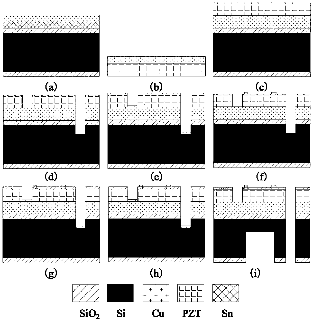
[0042] figure 2 It is the MEMS process flow chart of the entire device preparation. The process mainly includes the production of metal electrodes, the bonding of PZT piezoelectric ceramics and the substrate, the piezoelectric thick film process, the device patterning process and the release process of the cantilever beam. Fabrication of Micro Energy Harvester Based on Piezoelectric Thick Film MEMS Technology. Specific process flow:

[0043] (a) Electroplating 6um thick Cu and 6.5um thick Sn on a 4-inch silicon dioxide wafer (500um thick silicon in the middle, 500nm silicon dioxide on both sides) as a bonding layer and also a lower electrode layer;

[0044] (b) Plating Cu with a thickness of 6.5um on a 4-inch piezoelectric ceramic sheet as a bonding layer and also a lower electrode layer;

[0045] (c) Carry out eutectic bonding of the piezoelectric ceramic sheet and the silicon dioxide sheet that have been electroplated, and then mechanically thin, grind and polish the bond...


PUM

PropertyMeasurementUnit
thicknessaaaaaaaaaa

Abstract

The invention relates to the technical field of micro-energy collection, and discloses a micro-energy harvester based on a piezoelectric thick-film MEMS process and a preparation method thereof. The micro-energy harvester includes an upper electrode, a lower electrode, a silicon fixed base, a piezoelectric An electric cantilever beam and a quality block; one end of the piezoelectric cantilever beam is fixedly connected to the inner side wall of the silicon fixed base, and extends to the inner side wall on the other side opposite to the inner side wall; the piezoelectric cantilever The other end of the beam is fixedly connected to the suspended mass block; the upper electrode and the lower electrode are formed on a silicon fixed base, and the piezoelectric cantilever arm and the upper electrode cover the piezoelectric cantilever arm superior. The micro-energy harvester based on the piezoelectric thick film MEMS process and its preparation method can greatly improve the piezoelectric performance of the piezoelectric thick film, and can also prepare piezoelectric thick films, and can prepare device structures with more diversification and The advantages of higher complexity.

Description

technical field [0001] The invention relates to the technical field of micro-energy collection, in particular to a micro-energy collector based on piezoelectric thick-film MEMS technology and a preparation method thereof. Background technique [0002] MEMS (Micro-Electro-Mechanical System, Micro-Electro-Mechanical System) manufacturing technology is a general term for microstructure processing technology down to the nanometer scale and up to the millimeter scale. In a broad sense, the MEMS manufacturing technology is very rich in methods, almost involving various modern processing Technology, originated from semiconductor and microelectronics technology, uses lithography, epitaxy, film deposition, oxidation, diffusion, implantation, sputtering, evaporation, etching, scribing and packaging as basic process steps to manufacture complex three-dimensional shapes micromachining technology. [0003] In recent years, with the continuous development of wireless sensor network techn...

Claims


Application Information

Patent Timeline
Patent Type & Authority Patents(China)
IPC IPC(8): H01L41/113H01L41/25H01L41/312H02N2/18H10N30/30H10N30/03H10N30/072
CPCH02N2/18H10N30/306H10N30/03H10N30/072
Inventor 刘会聪杨湛陈涛孙立宁
Owner SUZHOU UNIV
Learn More