Transparent ultra-wideband microwave absorber based on transparent conductive film

A transparent conductive film, ultra-broadband technology, applied in electrical components, antennas, etc., can solve the problems of limiting the development of stealth microwave systems, poor absorbing performance, large size, etc., and achieve the effect of excellent absorption effect.

Inactive Publication Date: 2018-03-16
NANJING UNIV OF SCI & TECH
View PDF5 Cites 14 Cited by
  • Summary
  • Abstract
  • Description
  • Claims
  • Application Information

AI Technical Summary

Problems solved by technology

In recent years, the use of metamaterials to make microwave-absorbing materials has become a research hotspot. However, at present, traditional PCB boards are mostly used to make microwaves, which greatly limits the development of implicit microwave systems and is not suitable for military and medical applications.
Transparent microwaves can solve the above problems, but the existing transparent microwaves achieve microwave absorption through the superposition of simple conductive films, which have problems such as poor microwave absorption performance, narrow bandwidth, and large volume, and cannot be used in practical systems.

Method used


Image

  • Transparent ultra-wideband microwave absorber based on transparent conductive film
  • Transparent ultra-wideband microwave absorber based on transparent conductive film
  • Transparent ultra-wideband microwave absorber based on transparent conductive film

Examples


Embodiment 1

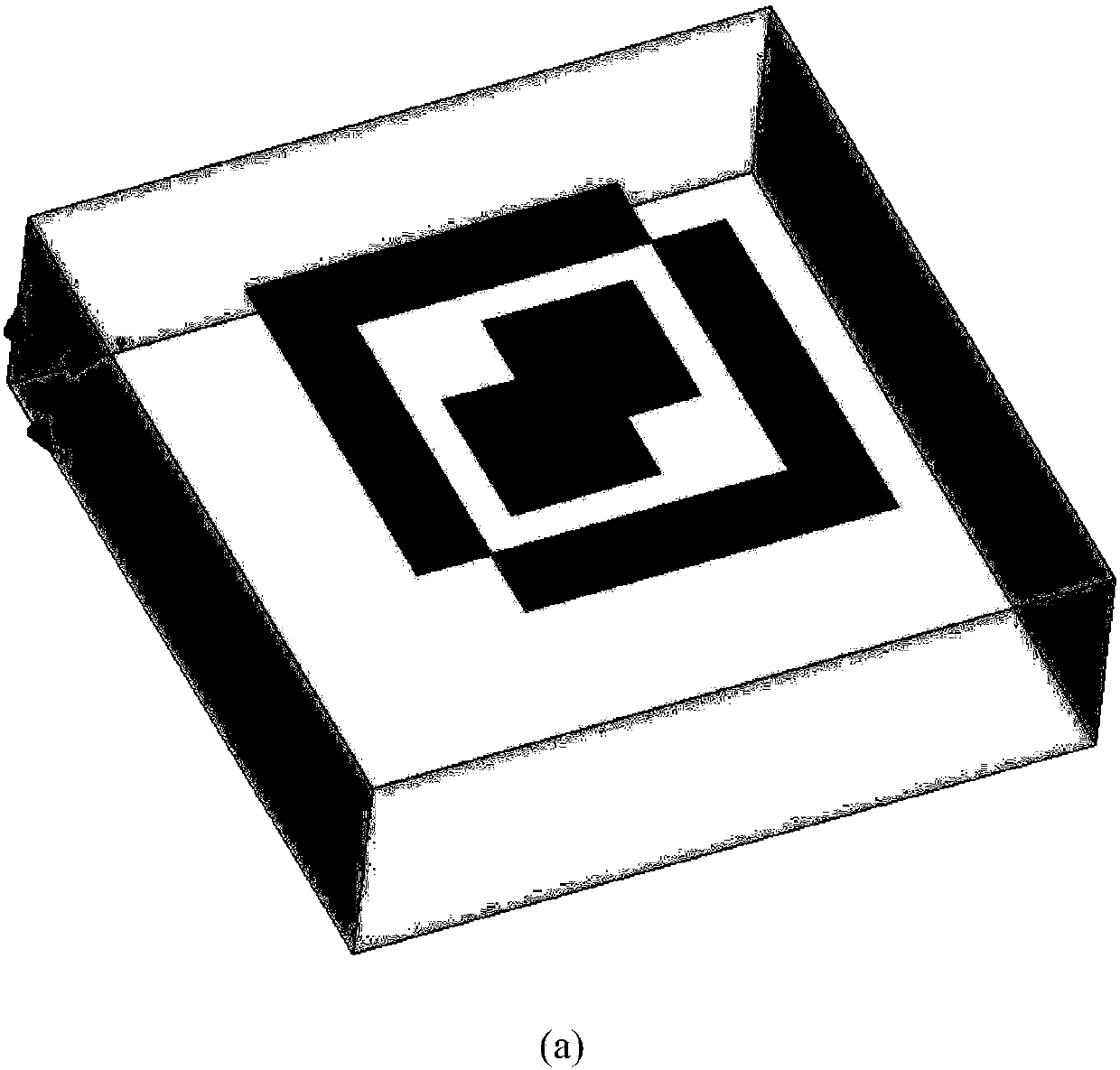
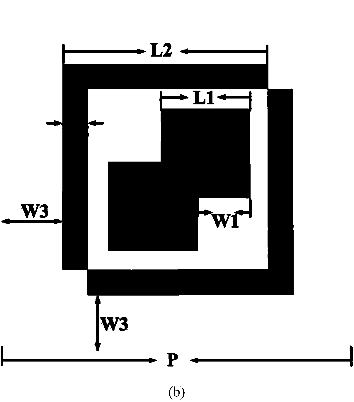
[0019] A transparent ultra-broadband microwave absorber based on a transparent conductive film, including glass and indium tin oxide film coated on both sides of the glass. The thickness of the microwave absorber is 1.1mm, and the film corresponding to the microwave incident surface is etched with a periodic structure. . A unit structure in a periodic structure such as figure 2 As shown, it consists of two overlapping squares. The side length of the square is 800um, and the overlapping part is 400um. The rectangular open ring surrounded by the outside has a side length of 2000um and a width of 400um. The size of the sample is 9.6mm*9.6mm, which contains a total of 576 unit structures in the above-mentioned 24 rows*24 columns. Under the electromagnetic wave of the frequency to be absorbed, the impedance of the absorbing structure and the impedance of the electromagnetic wave in free space achieve impedance matching.

[0020] image 3 for use figure 2 The comparison chart o...

Embodiment 2

[0025] Example 2 A series of experiments were carried out on the combined design of the center position of the wave-absorbing structural unit and the materials of the substrate and the conductive film. Side triangle, parallelogram, rectangle, square, cross or stripe structure, transparent conductive film includes indium tin oxide ITO, fluorine doped tin oxide FTO, zinc tin oxide ZTO, aluminum doped zinc oxide AZO, gallium tin oxide GTO, poly Ethylenedioxythiophene-polystyrene sulfonate PEDOT:PSS, graphene or carbon nanotube conductive film, the transparent medium is glass, polyimide PI, polyester PET, polynaphthalene and ethylene glycol ester PEN, Polyvinyl alcohol PVA, polydimethylsiloxane PDMS or polystyrene PS. In the experimental design, the specific size of the sample and each unit is adjusted. When a suitable periodic structure is selected to cooperate with the substrate and conductive film, the microwave broadband absorption effect can also be achieved.


PUM


Abstract

The invention discloses a transparent ultra-wideband microwave absorber based on a transparent conductive film. The transparent ultra-wideband microwave absorber comprises a transparent substrate andthe transparent conductive film which is coated on the two surfaces of the transparent substrate. Periodically distributed wave absorbing structures are etched on the corresponding film of the microwave incident surface. Impedance matching of the impedance of the wave absorbing structures and the impedance of electromagnetic waves in the free space can be realized under the electromagnetic waves of the unabsorbed frequency. The absorbing bandwidth of the wave absorber can be 23.4 GHz, the overall thickness is 1.1mm, the bandwidth is only 0.11 time of the corresponding wavelength of 32.5GHz center frequency and the microwave absorber is insensitive to the polarization angle.

Description

technical field [0001] The invention relates to microwave absorbing technology, in particular to a transparent ultra-broadband microwave absorber based on a transparent conductive film. Background technique [0002] Microwave absorbers play an important role in antenna design, filter structure, electromagnetic shielding, and electromagnetic compatibility. In recent years, the use of metamaterials to make microwave-absorbing materials has become a research hotspot. However, at present, traditional PCB boards are mostly used to make microwaves, which greatly limits the development of implicit microwave systems and is not suitable for military and medical applications. Transparent microwaves can solve the above problems, but the existing transparent microwaves achieve microwave absorption through the superposition of simple conductive films, which have problems such as poor microwave absorption performance, narrow bandwidth, and large volume, and cannot be used in practical sys...

Claims


Application Information

Patent Timeline
Patent Type & Authority Applications(China)
IPC IPC(8): H01Q17/00
CPCH01Q17/008
Inventor 顾文华赖森锋吴杨慧朱佳燚
Owner NANJING UNIV OF SCI & TECH
Why Eureka
Try Eureka