Multi-quantum well layer growing method of micro LED

A multi-quantum well layer and growth method technology, which is applied in the field of microLED multi-quantum well layer growth, can solve the problems of poor crystallization quality and poor electrical parameters of the quantum well layer structure, so as to improve antistatic ability and leakage performance, improve Effects of crystal quality and dislocation density reduction

Inactive Publication Date: 2018-03-23
HEFEI HUIKE JINYANG TECH
View PDF4 Cites 8 Cited by
  • Summary
  • Abstract
  • Description
  • Claims
  • Application Information

AI Technical Summary

Problems solved by technology

[0005] The purpose of the present invention is to solve the above technical problems, to provide a microLED multi-quantum well layer growth method, which

Method used


Image

  • Multi-quantum well layer growing method of micro LED
  • Multi-quantum well layer growing method of micro LED
  • Multi-quantum well layer growing method of micro LED

Examples


Example Embodiment

[0021] In order to make the objectives, technical solutions and advantages of the present invention clearer, the embodiments of the present invention will be further described in detail below with reference to the accompanying drawings.

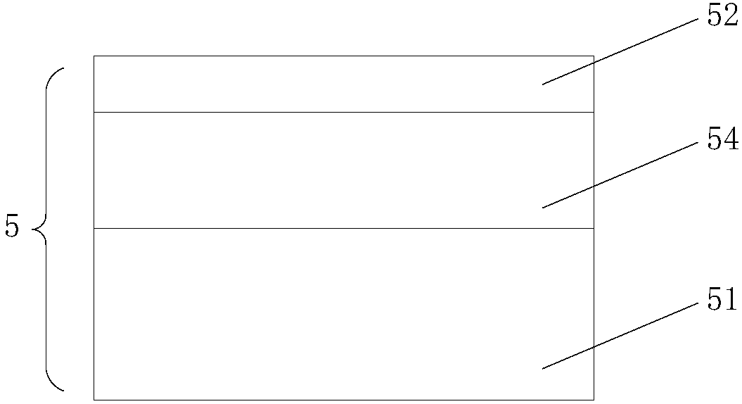
[0022] The present invention provides a method for growing a microLED multi-quantum well layer, see figure 1 , the multiple quantum well layer 5 includes a GaN barrier layer 51 and an In x Ga 1-x N well layer 52, 0x Ga 1-x During the process of the N well layer 52, hydrogen gas is not introduced.

[0023] The introduction of hydrogen gas during the formation of the microLED epitaxial structure can effectively improve the crystalline quality of GaN, but when growing the multiple quantum well layer, due to In x Ga 1-x The N well layer 52 contains In composition, and the introduction of hydrogen gas will destroy the In structure, thereby reducing the luminous efficiency. In the prior art, when the GaN barrier layer 51 is grown, the In x Ga ...


PUM


Abstract

The invention provides a multi-quantum well layer growing method of a micro LED. A multi-quantum well layer comprises a GaN barrier layer and an In<x>Ga<1-x>N well layer, wherein 0<X<1. Hydrogen is introduced in the process of forming the GaN barrier layer and hydrogen is not introduced in the process of forming the In<x>Ga<1-x>N well layer. According to the invention, by independently introducingthe hydrogen in the GaN barrier layer, the crystallization quality of the barrier layer is improved; stress between the GaN barrier layer and the In<x>Ga<1-x>N well layer; dislocation density is reduced; anti-static electricity ability and anti-electricity leakage performance of an epitaxial layer are improved; by further inserting a blocking layer between the GaN barrier layer and the In<x>Ga<1-x>N well layer, hydrogen possibly generated in the switching processes of growing the GaN barrier layer and the In<x>Ga<1-x>N well layer can be effectively prevented from overflowing to the In<x>Ga<1-x>N well layer to damage the In components; and the blocking layer is capable of allowing the In components to be quite uniformly distributed.

Description

technical field [0001] The invention relates to the technical field of microLEDs, in particular to a method for growing a microLED multi-quantum well layer. Background technique [0002] The display principle of MicroLED Display is to make the LED structure design into thin film, miniaturization, and array. On the transparent and opaque substrates; and then use the physical deposition process to complete the protective layer and the upper electrode, and then the upper substrate can be packaged to complete a Micro LED display with a simple structure. [0003] To make a display, the surface of the wafer must be made into an array structure like an LED display, and each pixel must be addressable and controllable, and driven to light up individually. If it is driven by a complementary metal oxide semiconductor circuit, it is an active addressing drive architecture. The MicroLED array chip and the CMOS can be packaged through packaging technology. After the paste is completed, t...

Claims


Application Information

Patent Timeline
IPC IPC(8): H01L33/06H01L33/14H01L33/32H01L33/00
CPCH01L33/06H01L33/0075H01L33/14H01L33/32
Inventor 白航空
Owner HEFEI HUIKE JINYANG TECH
Why Eureka
Try Eureka