Chip sintered product, sub unit, IGBT packaging module and preparation method

A technology for encapsulating modules and sintered products, which is applied in the fields of IGBT packaged modules and their preparation, chip sintered products, subunits, press-fit IGBT packaged modules and their preparations, and can solve the problems of reducing thermal resistance, poor thermal interface layer compactness, shear Low shear strength and other problems, to achieve the effect of reducing thermal resistance, increasing shear strength, and improving dispersibility

Active Publication Date: 2018-03-27
GLOBAL ENERGY INTERCONNECTION RES INST CO LTD +2
View PDF4 Cites 7 Cited by
  • Summary
  • Abstract
  • Description
  • Claims
  • Application Information

AI Technical Summary

Problems solved by technology

[0006] For this reason, the thermal interface layer in the existing IGBT module to be solved by the present invention has the defects of poor compactness, low shear strength and insufficient ability to reduce thermal res

Method used


Image

  • Chip sintered product, sub unit, IGBT packaging module and preparation method
  • Chip sintered product, sub unit, IGBT packaging module and preparation method
  • Chip sintered product, sub unit, IGBT packaging module and preparation method

Examples


preparation example Construction

[0060] In the preparation process of the IGBT package module, the pressure sintering equipment of the model Auto-F-XL-HC manufactured by boschman can be used in the pressure sintering process.

[0061] Chip sintered products:

Embodiment 1

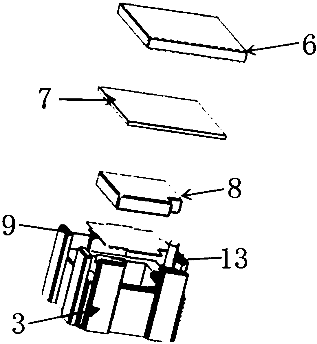
[0063] This embodiment provides a chip sintered product, including a first molybdenum sheet and a second molybdenum sheet and a chip 7 arranged between them, at least one of the first molybdenum sheet and the second molybdenum sheet is a prefabricated molybdenum sheet The prefabricated molybdenum sheet is a molybdenum sheet with a prefabricated nano-silver film 14 on the surface, and at least one side of the chip 7 is in contact with the prefabricated nano-silver film 14 .

[0064] In the present embodiment, the first molybdenum sheet is a prefabricated molybdenum sheet, which is obtained by pressing the prefabricated nano-silver film 14 on the upper molybdenum sheet 6, and the second molybdenum sheet is a non-prefabricated molybdenum sheet, that is, the lower molybdenum sheet 8; In another embodiment, both the first molybdenum sheet and the second molybdenum sheet are prefabricated molybdenum sheets.

[0065] In the above chip sintering products, the use of prefabricated nano...

Embodiment 2

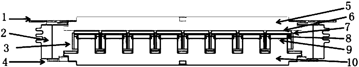
[0076] This embodiment provides a chip subunit 15, such as image 3 As shown, including the chip sintered product in embodiment 1;

[0077] The metal support sheet is in contact with the lower molybdenum sheet 8 and is used to support the chip sintered product; in the present embodiment, the metal support sheet is a silver sheet 9;

[0078] The subunit frame 3 has an opening at one end, and a support unit suitable for supporting the metal support sheet is arranged in it; in this embodiment, the support unit can specifically be provided with a groove on the inner peripheral wall of the subunit frame 3 close to the opening, The groove is suitable for the metal support sheet to be stuck on it through the opening, and the subunit frame 3 is made of PEAK material; The shaft extends perpendicular to the inner wall, and the metal support sheet can be placed on the support shaft;

[0079] A connection unit, one end of which is in contact with the grid on the chip, to ensure its elec...


PUM

PropertyMeasurementUnit
Thicknessaaaaaaaaaa
The average diameteraaaaaaaaaa
Thicknessaaaaaaaaaa

Abstract

The invention discloses a chip sintered product, a sub unit, an IGBT packaging module and a preparation method. The chip sintered product comprises a first molybdenum sheet, a second molybdenum sheetand a chip placed between the first and second molybdenum sheets; at least one of the first and second molybdenum sheets is a prefabricated molybdenum sheet; the prefabricated molybdenum sheet is a molybdenum sheet with a prefabricated nanometer silver film on the surface; in addition, at least one surface of the chip is in contact with the prefabricated nanometer silver film; by adoption of the prefabricated nanometer silver film, distribution uniformity of nanometer silver particles in the subsequent pressuring and sintering process can be improved effectively, a "coffee ring effect" can beavoided, and thermal resistance can be lowered; meanwhile, it is ensured that nano-scale holes are uniformly distributed in a sintering layer obtained by sintering, and by virtue of the nano-scale holes, stress generated between the chip and the molybdenum sheet can be lowered effectively, and the shearing strength of the chip sintered product is improved; and by adoption of the chip sintered product and the IGB packaging module with low thermal resistance and high shearing strength, the sintering layer obtained by sintering the prefabricated nanometer silver film has high compactness, and thenano-scale holes are distributed.

Description

technical field [0001] The invention belongs to the technical field of IGBT packaging module packaging, and specifically relates to a chip sintered product, a subunit, an IGBT packaging module and a preparation method thereof, in particular to a chip sintered product, a subunit, and a crimping type IGBT packaging module using a nano-silver film and its preparation method. Background technique [0002] As a new generation of fully-controlled power electronic devices, the IGBT module has become a mainstream device in the field of power electronics after more than 30 years of rapid development. Smart grid and other fields are rapidly promoted. [0003] IGBT modules are generally divided into crimp-type IGBT modules and solder-type IGBT modules. Compared with the traditional soldered IGBT module, the press-fit IGBT module has the following advantages: 1) The chip layout is denser, the module current density is higher, and it is easy to achieve high current; 2) The internal lea...

Claims


Application Information

Patent Timeline
IPC IPC(8): H01L23/488H01L25/16H01L21/603
CPCH01L24/29H01L24/83H01L25/162H01L25/165H01L2224/2918H01L2224/83203
Inventor 田丽纷李现兵张朋武伟林仲康石浩张喆唐新灵王亮
Owner GLOBAL ENERGY INTERCONNECTION RES INST CO LTD
Why Eureka
Try Eureka