Lithium ion battery silicon-tin composite negative electrode material and preparation method thereof
A technology for lithium-ion batteries and negative electrode materials, applied in battery electrodes, secondary batteries, circuits, etc., can solve the problems of poor electrical conductivity, crushing, pulverization, and falling off of silicon
- Summary
- Abstract
- Description
- Claims
- Application Information
AI Technical Summary
Problems solved by technology
Method used
Image
Examples
Embodiment 1
[0027] Preparation of plating solution: SnCl 2 75g / L, NaOH100g / L, sodium citrate 233g / L;
[0028] Electroless plating time: 5min
[0029] Chemical plating temperature: 50℃
[0030] Stirring conditions: 300 revolutions per minute / min
[0031] Post-processing: After the electroless plating product is cleaned and filtered with deionized water, it is dried in a blast oven to obtain a silicon-tin composite material with a silicon content of 73.9% and a tin content of 26.1%; this material is Negative electrode material, assembled button cell, conductive agent is acetylene black, binder is PVDF; silicon-tin active material, the mass ratio of conductive agent and binder is 70:15:15; charge and discharge current density is 100mA / g.
[0032] figure 1 SEM image of the silicon-tin composite material in Example 1 (scanning electron microscope model: Hitachi S-4800)
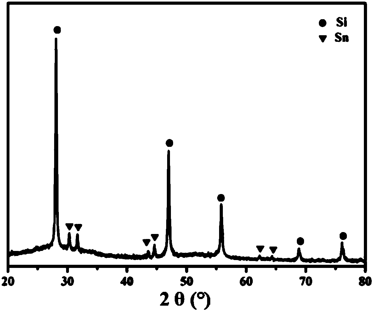
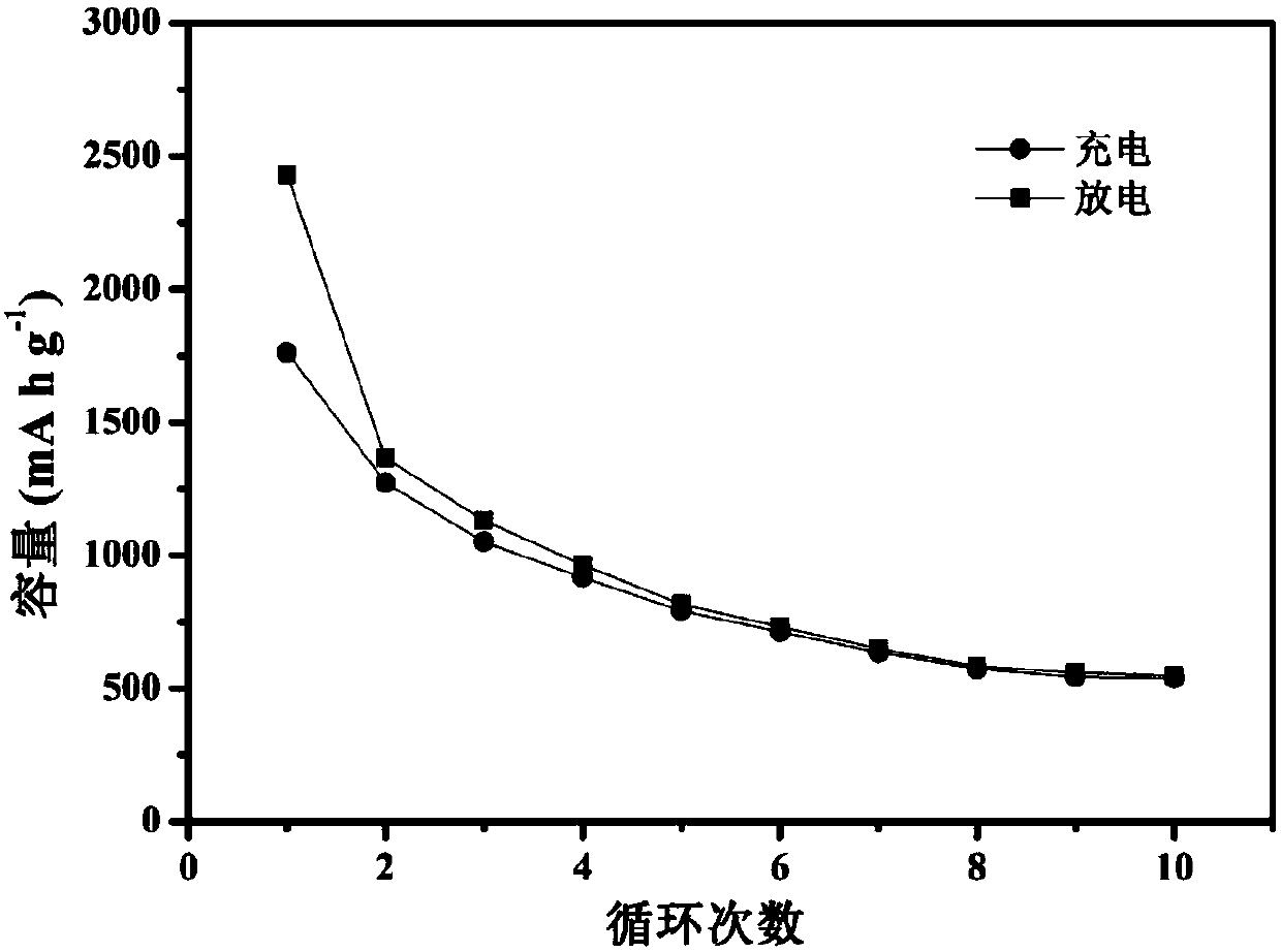
[0033] figure 2 For the XRD pattern of silicon in Example 1, it can be determined that Si and Sn are present in the material (X-ray d...
Embodiment 2
[0036] Preparation of plating solution: SnCl 2 70g / L, NaOH120g / L, sodium citrate 200g / L;
[0037] Electroless plating time: 8min
[0038] Chemical plating temperature: 80℃
[0039] Stirring conditions: 200 revolutions per minute / min
[0040] Post-processing: After cleaning and filtering the chemically plated product with deionized water, it is dried in a blast oven to obtain a silicon-tin composite material with a silicon content of 55% and a tin content of 45%; this material is Negative electrode material, assembled button cell, conductive agent is acetylene black, binder is PVDF; silicon-tin active material, the mass ratio of conductive agent and binder is 70:15:15; charge and discharge current density is 100mA / g.
[0041] Figure 4 SEM image of the silicon-tin composite material in Example 2 (scanning electron microscope model: Hitachi S-4800)
[0042] Figure 5 For the XRD pattern of silicon in Example 2, it can be determined that Si and Sn are present in the material (X-ray diffrac...
Embodiment 3
[0045] Preparation of plating solution: SnCl 2 75g / L, NaOH 110g / L, sodium citrate 220g / L;
[0046] Electroless plating time: 2min
[0047] Chemical plating temperature: 75℃
[0048] Post-processing: After the electroless plating product is cleaned and filtered with deionized water, it is dried in a blast oven to obtain a silicon-tin composite material with a silicon content of 52.6% and a tin content of 47.4%; this material is Negative electrode material, assembled button cell, conductive agent is acetylene black, binder is PVDF; silicon-tin active material, the mass ratio of conductive agent and binder is 70:15:15; charge and discharge current density is 100mA / g.
[0049] Figure 7 SEM image of the silicon-tin composite material in Example 3 (scanning electron microscope model: Hitachi S-4800)
[0050] Picture 8 For the XRD pattern of silicon in Example 3, it can be determined that Si and Sn are present in the material (X-ray diffractometer model: Rigaku D / MAX-2500)
[0051] Picture...
PUM
| Property | Measurement | Unit |
|---|---|---|
| Particle size | aaaaa | aaaaa |
| Charge and discharge current density | aaaaa | aaaaa |
Abstract
Description
Claims
Application Information


