Cuprous oxide semiconductor ceramic material and preparation method thereof

A ceramic material, cuprous oxide technology, applied in the field of cuprous oxide semiconductor ceramic materials and its preparation, can solve the problems of semiconductor ceramic material damage, failure, electrical corrosion resistance, chemical corrosion resistance and other problems, and achieve long service life , good constructability and good comprehensive performance

Active Publication Date: 2018-03-30
SHAANXI AVIATION ELECTRICAL
View PDF6 Cites 1 Cited by
  • Summary
  • Abstract
  • Description
  • Claims
  • Application Information

AI Technical Summary

Problems solved by technology

However, Cu is directly used in the raw material 2 The cuprous oxide semiconductor ceramic material prepared by O has insufficient electrical corrosion resistance and

Method used


Image

  • Cuprous oxide semiconductor ceramic material and preparation method thereof
  • Cuprous oxide semiconductor ceramic material and preparation method thereof
  • Cuprous oxide semiconductor ceramic material and preparation method thereof

Examples


Embodiment Construction

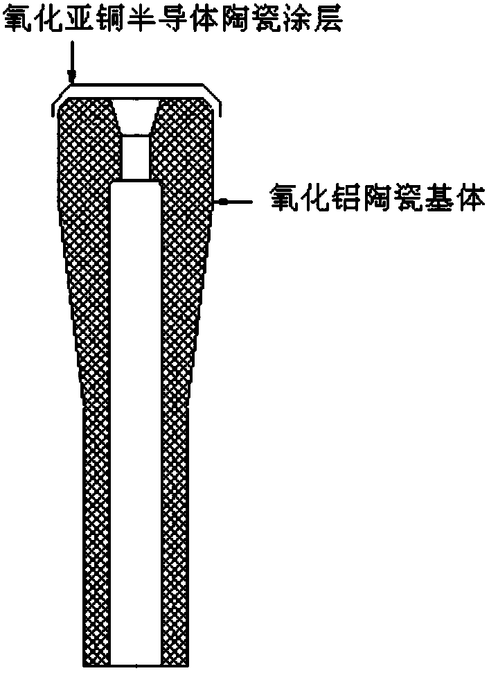
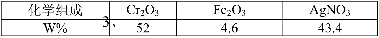
[0020] A cuprous oxide semiconductor ceramic material, the composition of the cuprous oxide semiconductor ceramic material includes copper oxide, copper powder, ferric oxide, chromium oxide, silver nitrate, mullite, quartz sand, spinel ; wherein the proportion of copper oxide is 25% to 39.8%, the proportion of copper powder is 15% to 25.4%, the proportion of ferric oxide is 0.5% to 0.8%, the proportion of dichromium oxide is 5% to 9%, The proportion of silver nitrate is 5%-7.5%, the proportion of mullite is 5%-7%, the proportion of quartz sand is 1%-5.5%, and the proportion of spinel is 1%-5%.

[0021] A preparation method of cuprous oxide semiconductor ceramic material, said method takes the following steps:

[0022] 1) The raw materials of copper oxide, copper powder, ferric oxide, chromium oxide, silver nitrate, mullite, quartz sand, and spinel are calcined and pretreated respectively, and sieved;

[0023] 2) Weigh and mix the sieved materials respectively, so that the pro...


PUM


Abstract

The invention relates to a cuprous oxide semiconductor ceramic material and a preparation method of the material and belongs to the technical field of functional materials. The invention provides a novel formula of the cuprous oxide semiconductor ceramic material. According to the formula, direct adoption of a Cu2O raw material formerly is changed; and other metal oxide raw materials are added asingredients on the basis of Cu2O. The composition formula of the semiconductor ceramic material is changed; metal oxides improving conductivity are selected to reduce volume resistance of the semiconductor ceramic material; the electrocorrosion resistance and chemical corrosion resistance of the semiconductor ceramic material are improved; the bonding strength of the semiconductor ceramic materialwith Al2O3 and ZrO2 base materials is improved; and therefore, a service life of the semiconductor ceramic material is prolonged. At the same time, the threats to personnel and an environment are reduced in a preparation process.

Description

technical field [0001] The invention discloses a cuprous oxide semiconductor ceramic material and a preparation method thereof, belonging to the technical field of functional materials. Background technique [0002] According to the difference between the semiconductor materials used in the discharge end of the semiconductor nozzle of the aircraft engine, the semiconductor nozzle is divided into two categories: the first type is the semiconductor glaze type (coating) nozzle, and the discharge terminal is Al 2 o 3 , ZrO 2 As the substrate, the substrate is coated with more Cu 2 O-based semiconductor ceramic materials are fired after firing; the second type is semiconductor block type nozzles, that is, the discharge end directly uses SiC, SnO 2 And other materials are directly pressed into shape. Semiconducting ceramics have inhomogeneity and a negative temperature coefficient of resistance. When an external voltage is applied, several electrical conductions are formed, a ...

Claims


Application Information

Patent Timeline
IPC IPC(8): C04B35/45C04B35/622
CPCC04B35/45C04B35/622C04B2235/3222C04B2235/3241C04B2235/3272C04B2235/3418C04B2235/3463C04B2235/443C04B2235/6567C04B2235/9607
Inventor 乌凯万思明
Owner SHAANXI AVIATION ELECTRICAL
Why Eureka
Try Eureka