

Transverse power device high-voltage interconnection structure
A technology of lateral power devices and interconnection structures, which is applied in the direction of semiconductor devices, electrical components, circuits, etc., can solve the problems of increasing process complexity and achieve the effects of low cost, enhanced withstand voltage capability, and simple process preparation
- Summary
- Abstract
- Description
- Claims
- Application Information
AI Technical Summary
Problems solved by technology
Method used
Image

Examples
Embodiment 1
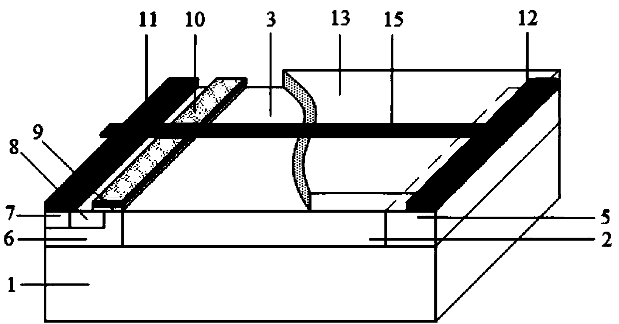
[0040] Such as Figure 4a Shown is a schematic diagram of a three-dimensional structure of a lateral power device with a high-K insulating region provided by the present invention, Figure 4b is along Figure 4a The cross-sectional view of the device along the AB line. It can be seen that a trench of a certain shape is etched on the epitaxial layer 2 , and then an insulating material with a high dielectric constant is filled in the trench, thereby forming a semiconductor region 3 and a high-K insulator region 4 . Next, a semiconductor drain region 5, a semiconductor body region 6, a semiconductor body contact region 7, a semiconductor source region 8, a gate oxide layer 9, a gate metal 10, a source metal 11, Drain metal 12, insulating dielectric layer 13, high-voltage interconnection metal wire 15.
Embodiment 2
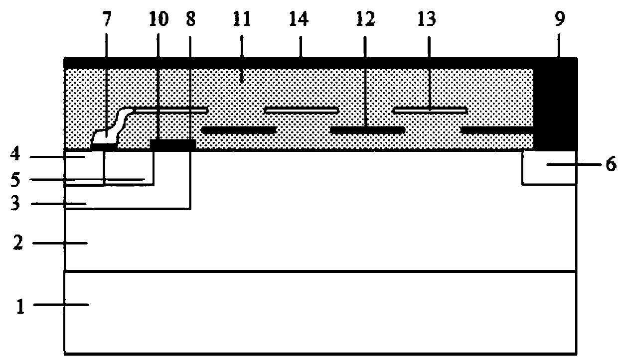
[0042] Under the condition that the basic structure remains unchanged, a flexible design is carried out, Figure 5a It is a high-voltage interconnection LDMOS with a high-K insulator region and a low-K insulating dielectric region provided by the present invention, Figure 5b is along Figure 5a The cross-sectional view of the device along the AB line. It can be seen from the figure that the insulating dielectric layer 13 in the area directly above the high-K insulator region 4 is a low-K insulating dielectric layer 14 made of a low-K material, while the insulating dielectric layer above the semiconductor region 3 in the drift region still uses is conventional silica.
Embodiment 3
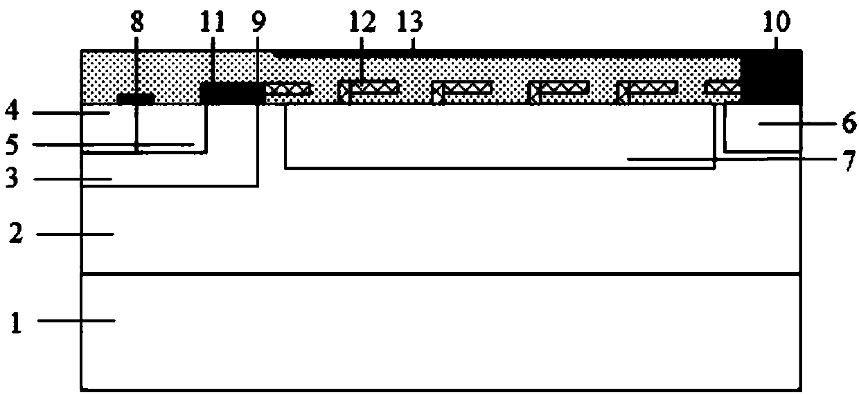
[0044] Under the condition that the basic structure remains unchanged, a flexible design is carried out, Figure 6a It is a high-voltage interconnection LDMOS with a high-K insulating region and an extended low-K insulating dielectric region provided by the present invention, Figure 6b is along Figure 6a The cross-sectional view of the device along the AB line. It can be seen from the figure that the drift region of this structure is composed of a semiconductor region 3, a high-K insulating region 4, and a low-K insulating dielectric layer 14 above it. The thickness of the low-K insulating dielectric layer 14 is thicker than that of the insulating dielectric layer 13, and extends High-K insulator region 4. The insulating dielectric layer above the semiconductor region 3 is still conventional silicon dioxide.
PUM
 Abstract
Description
Claims
Application Information