Photoelectric cathode and preparation method thereof
A photocathode, p-type technology, used in the manufacture of light-emitting cathodes, photo-emission cathodes, main electrodes of discharge tubes, etc., can solve the problems of poor conductivity, low conductivity, and low quantum efficiency of non-activation photocathodes
- Summary
- Abstract
- Description
- Claims
- Application Information
AI Technical Summary
Problems solved by technology
Method used
Image
Examples
Embodiment 1
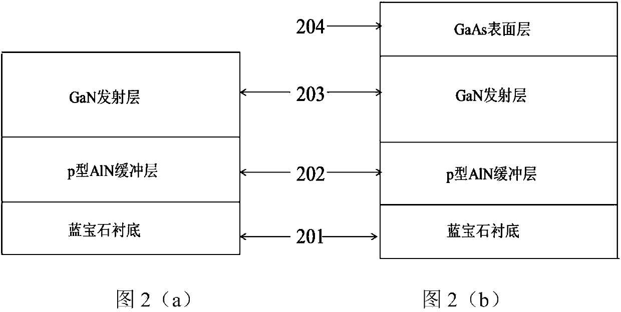
[0055] A photocathode, its optical structure and Al component structure diagram as shown in figure 2 As shown in (b), it includes a sapphire substrate 201, a p-type doped AlN buffer layer 202 formed on the sapphire substrate 201, a p-type GaN emission layer 203 formed on the p-type doped AlN buffer layer 202, and a p-type GaN emission layer formed on the The intrinsic type GaAs surface layer 204 on the p-type GaN emitter layer 203 .
[0056] Its preparation method comprises the following steps:
[0057] 1) A p-type AlN buffer layer 202 with a thickness of 200 nm is grown on a double-sided polished sapphire substrate 201 with a thickness of 0.46 mm by MOCVD epitaxial growth method, and the dopant atom is Mg, and the doping concentration is 1×10 16 cm -3 ;
[0058] 2) Using the MOCVD epitaxial growth method and the p-type doping process of semiconductor materials, grow p-type Al on the p-type AlN buffer layer 202 x Ga 1-x N emitter layer, where p-type Al x Ga 1-x The numb...
Embodiment 2
[0075] A photocathode, its optical structure and Al component structure diagram as shown in image 3 As shown, it includes a sapphire substrate 301, a p-type AlN buffer layer 302 formed on the sapphire substrate 301, a p-type GaN emission layer 303 formed on the p-type AlN buffer layer 302, and a p-type GaN emission layer 303 formed on the p-type GaN emission layer 303. The intrinsic type InP surface layer 304.
[0076] Its preparation method comprises the following steps:
[0077] 1) A p-type AlN buffer layer 302 with a thickness of 200 nm is grown on a double-sided polished sapphire substrate 301 with a thickness of 0.46 mm by MOCVD epitaxial growth method, and the dopant atom is Mg, and the doping concentration is 1×10 16 cm -3 ;
[0078] 2) Using the MOCVD epitaxial growth method and the p-type doping process of semiconductor materials, grow p-type Al on the p-type AlN buffer layer 302 x Ga 1-x N emitter layer, where p-type Al x Ga 1-x The number of sub-layers of th...
Embodiment 3
[0084] A photocathode, its optical structure and Al component structure diagram as shown in image 3 As shown, it includes a sapphire substrate 401, a p-type AlN buffer layer 402 formed on the sapphire substrate 401, and a p-type AlN buffer layer 402 formed on the p-type AlN buffer layer. 0.9 Ga 0.1 N emitter layer 403, formed on p-type Al 0.9 Ga 0.1 p-type Al on N emitter layer 403 0.65 Ga 0.35 N emitter layer 404, formed on p-type Al 0.65 Ga 0.35 A p-type GaN emission layer 405 on the N emission layer 404 and an intrinsic type GaAs surface layer 407 formed on the p-type GaN emission layer 405 .
[0085] Its preparation method comprises the following steps:
[0086] 1) A p-type AlN buffer layer 402 with a thickness of 200 nm is grown on a double-sided polished sapphire substrate 401 with a thickness of 0.46 mm by MOCVD epitaxial growth method, and the dopant atom is Mg, and the doping concentration is 1×10 16 cm -3 ;
[0087] 2) Using the MOCVD epitaxial growth meth...
PUM
 Abstract
Description
Claims
Application Information


