Processing method of nanometer-sized and micron-sized holes

A processing method, nanotechnology, applied in the direction of nanotechnology, technology for producing decorative surface effects, microstructure technology, etc., to achieve the effects of shape and depth controllable, large application value, and environmentally friendly operation

Active Publication Date: 2018-05-01
GUANGDONG UNIV OF TECH +1
View PDF3 Cites 9 Cited by
  • Summary
  • Abstract
  • Description
  • Claims
  • Application Information

AI Technical Summary

Problems solved by technology

Correspondingly, the diameter of the nanopores formed by the processing is also strictly limited to 10nm-100nm
In addition, since the gold nanoparticles are affected by the evaporation of the substrate during processing, their trajectory has a certain degree of randomness. Therefore, how to control the trajectory of the gold nanoparticles during processing and then process the pores with controllable shapes is extremely challenging.

Method used


Image

  • Processing method of nanometer-sized and micron-sized holes
  • Processing method of nanometer-sized and micron-sized holes
  • Processing method of nanometer-sized and micron-sized holes

Examples


Embodiment 1

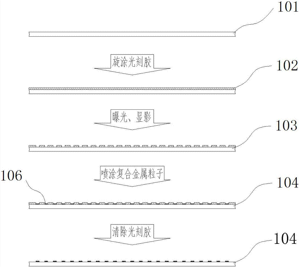
[0035] Step 1: Clean the substrate 101 with deionized water, and remove the surface dirt with a plasma cleaner; the substrate 101 is a plate-shaped material of polyethylene terephthalate (PET);

[0036] Step 2: If figure 1 As shown, the photoresist 102 is spin-coated on the substrate 101, exposed and developed to form a specific substrate 103 printed with a target pattern;

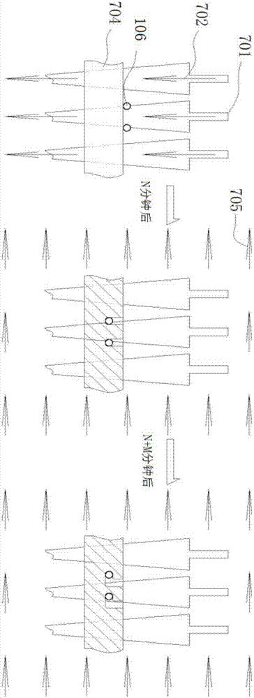
[0037] Step 3: Deposit micro-nano composite structure metal particles 106 on the substrate surface, that is, control the area of ​​the micro-nano composite structure metal particles 106 deposited on the substrate surface according to the exposed pattern, and then control the shape of the nanopore or micropore (such as a circle shape, square, etc.) and aperture; the micro-nano composite metal particle 106 is centered on the magnetic core, and the surface of the magnetic core is plated with a nano-metal particle coating composed of a plurality of nano-gold, silver or aluminum particles; the magnetic The core ...

Embodiment 2

[0042] Step 1: Clean the substrate 101 with deionized water, and remove the surface dirt with a plasma cleaner; the substrate 101 is a glass plate material;

[0043] Step 2: Spin-coat the photoresist 102 on the substrate 101, expose and develop, and form a specific substrate 103 printed with target patterns;

[0044] Step 3: Deposit micro-nano composite structure metal particles 106 on the substrate surface, that is, control the area of ​​the micro-nano composite structure metal particles 106 deposited on the substrate surface according to the exposed pattern, and then control the shape of the nanopore or micropore (such as a circle shape, square, etc.) and aperture; the micro-nano composite metal particle 106 is centered on the magnetic core, and the surface of the magnetic core is plated with a nano-metal particle coating composed of a plurality of nano-gold, silver or aluminum particles; the magnetic The core is spherical iron particles, nickel particles, cobalt particles a...

Embodiment 3

[0049] Step 1: Clean the substrate 101 with deionized water, and remove the surface dirt with a plasma cleaner; the substrate 101 is a glass plate material;

[0050] Step 2: Spin-coat the photoresist 102 on the substrate 101, expose and develop, and form a specific substrate 103 printed with target patterns;

[0051] Step 3: Deposit micro-nano composite structure metal particles 106 on the substrate surface, that is, control the area of ​​the micro-nano composite structure metal particles 106 deposited on the substrate surface according to the exposed pattern, and then control the shape of the nanopore or micropore (such as a circle shape, square, etc.) and aperture; the micro-nano composite metal particle 106 is centered on the magnetic core, and the surface of the magnetic core is plated with a nano-metal particle coating composed of a plurality of nano-gold, silver or aluminum particles; the magnetic The core is spherical iron particles, nickel particles, cobalt particles a...


PUM

PropertyMeasurementUnit
radiusaaaaaaaaaa
diameteraaaaaaaaaa
lengthaaaaaaaaaa

Abstract

The invention relates to a processing method of nanometer-sized and micron-sized holes, which comprises the following steps: (1) a base material is cleaned, and dirt on the surface is removed; (2) photoresist is spin-coated, and after exposure and development, a substrate is formed; (3) micro-nano composite structure metal particles are deposited on the surface of the substrate; and with a magnetic core as a center, the surface of the micro-nano composite structure metal particle is plated with a metal nanoparticle plating composed of a plurality of nano-gold, -silver or -aluminium particles;(4) the photoresist is removed with only a micro-nano composite structure metal particle dot array left; (5) laser is adopted to irradiate the substrate while a uniform strong magnetic field is applied, so that processed holes are formed by processing; (6) after nanometer-sized holes or micron-sized holes with a target hole diameter, shape and depth are achieved, laser irradiation is stopped and the uniform magnetic field is removed, and thereby a finished product is obtained. The processing method proposed by the invention can process blind holes or through holes with a hole diameter being 100nm or more and any nanometer-sized shape, is environmentally friendly, and is easy to operate, and the processed hole diameter, shape and depth can all achieve a controllable effect.

Description

technical field [0001] The invention relates to the technical field of material processing, in particular to a processing method for nanometer and micrometer holes. Background technique [0002] With the continuous improvement of micro-nano processing technology, the micro-nano structure with smaller structure size and higher precision requirements can be realized. For example, solid-state nanopores for single-molecule analysis of DNA are one of the typical cases. Compared with biological nanopores commonly used in DNA single-molecule analysis, solid-state nanopores have obvious advantages in chemical, thermal, and mechanical stability, and can be fabricated by conventional micro-nano processing techniques, so that nanopores can be realized large-scale processing, and can precisely control its pore size. Therefore, many research groups continue to focus on the processing of solid-state nanopores and study the movement of biomolecules in solid-state nanopores. [0003] The...

Claims


Application Information

Patent Timeline
Patent Type & Authority Applications(China)
IPC IPC(8): B81C1/00B82Y40/00
CPCB81C1/00349B81C1/00412B81C1/00849B82Y40/00H01L21/30604B81C1/00087B81C2201/0188B81C1/00373H01L29/0665
Inventor 陈新施达创陈云高健汪正平杨海东
Owner GUANGDONG UNIV OF TECH
Why Eureka
Try Eureka