

Preparation method of field effect transistor based on two-dimensional gallium selenide material
A field effect transistor, target material technology, applied in semiconductor devices, final product manufacturing, sustainable manufacturing/processing, etc., can solve problems such as low preparation efficiency, and achieve the effect of simple method, reduced process steps, and easy operation
- Summary
- Abstract
- Description
- Claims
- Application Information
AI Technical Summary
Problems solved by technology
Method used
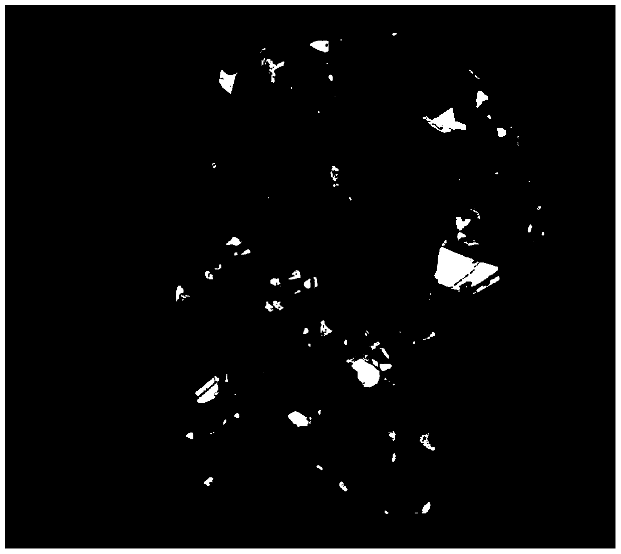
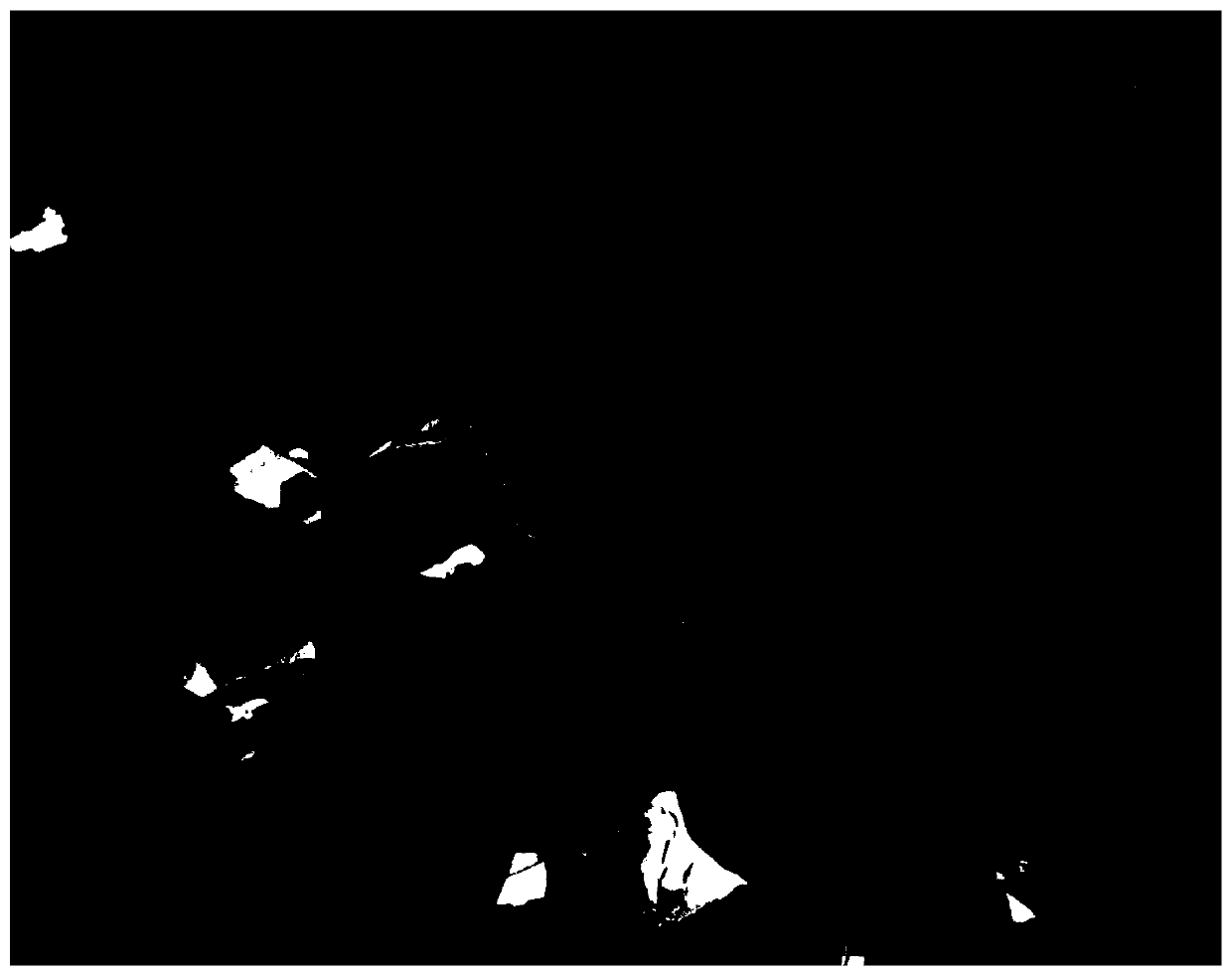
Image


Examples
Embodiment 1
[0027] Step 1. A high-quality GaSe single crystal is grown by the vertical Bridgman method, a GaSe bulk material with a smooth surface and no defects is selected, and a GaSe thin layer with a thickness of 15 μm is obtained by cleavage along its cleavage plane.
[0028] Step 2: Attach the GaSe thin layer to the Scotch tape evenly, fold the tape in half and tear it off quickly, and repeat the operation 6 times until the material on the tape is dull and colorless.
[0029] Step 3: Adhere the tape with the GaSe material evenly to PDMS (polydimethylsiloxane) with a thickness of 0.5 mm, and peel off the PDMS to obtain two-dimensional GaSe materials with different thicknesses. To obtain thinner GaSe materials, the tape should be peeled off quickly in one direction.
[0030] Step 4: Under an optical microscope, find a two-dimensional GaSe with a uniform thickness and a size of 30 μm×60 μm as a target material for transfer. Use a puncher to punch a round hole with a diameter of 3mm on...
Embodiment 2
[0040] Step 1. A high-quality GaSe single crystal is grown by the vertical Bridgman method, a GaSe bulk material with a smooth surface and no defects is selected, and a GaSe thin layer with a thickness of 10 μm is obtained by cleavage along its cleavage plane.
[0041] Step 2: Attach the GaSe thin layer to the Scotch tape evenly, fold the tape in half and tear it off quickly, repeat the operation 8 times until the material on the tape is dull and colorless.
[0042] Step 3: Adhere the tape with the GaSe material evenly to PDMS (polydimethylsiloxane) with a thickness of 0.5 mm, and peel off the PDMS to obtain two-dimensional GaSe materials with different thicknesses. To obtain thinner GaSe materials, the tape should be peeled off quickly in one direction.
[0043] Step 4: Under an optical microscope, find a two-dimensional GaSe with a uniform thickness and a size of 6 μm×21 μm as a target material for transfer. Punch a circular hole with a diameter of 2mm on the tape with a pu...
Embodiment 3
[0052] Step 1. A high-quality GaSe single crystal is grown by the vertical Bridgman method, a GaSe bulk material with a smooth surface and no defects is selected, and a GaSe thin layer with a thickness of 13 μm is obtained by cleavage along its cleavage plane.
[0053] Step 2: Attach the GaSe thin layer to the Scotch tape evenly, fold the tape in half and tear it off quickly, repeat the operation 7 times until the material on the tape is dull and colorless.
[0054] Step 3: Adhere the tape with the GaSe material evenly to PDMS (polydimethylsiloxane) with a thickness of 0.5 mm, and peel off the PDMS to obtain two-dimensional GaSe materials with different thicknesses. To obtain thinner GaSe materials, the tape should be peeled off quickly in one direction.
[0055] Step 4: Under an optical microscope, find a two-dimensional GaSe with a uniform thickness and a size of 12 μm×18 μm as a target material for transfer. Punch a round hole with a diameter of 2.5mm on the tape with a pu...
PUM
| Property | Measurement | Unit |
|---|---|---|
| thickness | aaaaa | aaaaa |
Abstract
Description
Claims
Application Information