Integrated packaging structure of IGBT chip and phase-transformation soaking plate

An integrated packaging and vapor chamber technology, which is applied in semiconductor/solid-state device manufacturing, electrical components, and electrical solid-state devices. The effect of enhancing heat exchange efficiency

Pending Publication Date: 2018-05-11
SOUTH CHINA UNIV OF TECH +1
View PDF1 Cites 6 Cited by
  • Summary
  • Abstract
  • Description
  • Claims
  • Application Information

AI Technical Summary

Problems solved by technology

[0005] In view of the technical problems existing in the prior art, one of the purposes of the present invention is to provide an integrated packaging structure of the IGBT chip and the phase-change vapor chamber, which can eliminate the hot spot phenomenon of the IGBT chip and solve the problem of the IGBT chip and the vapor chamber. The problem of large indirect contact thermal resistance can improve the heat dissipation efficiency of the device, and the structure layout is reasonable, which is convenient for manufacturing
[0006] Aiming at the technical problems existing in the prior art, the second purpose of the present invention is to provide a manufacturing method of an integrated packaging structure of an IGBT chip and a phase-change vapor chamber, so that it can solve the problem of heat soaking when the IGBT chip is welded on the vapor chamber. The pressure inside the plate is too high and there is a problem of bulging

Method used


Image

  • Integrated packaging structure of IGBT chip and phase-transformation soaking plate
  • Integrated packaging structure of IGBT chip and phase-transformation soaking plate
  • Integrated packaging structure of IGBT chip and phase-transformation soaking plate

Examples


Embodiment Construction

[0043] The present invention will be described in further detail below.

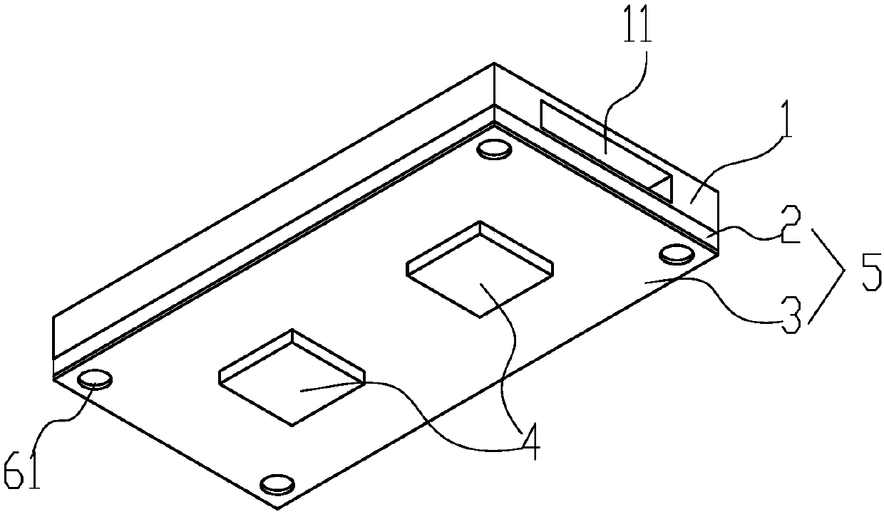
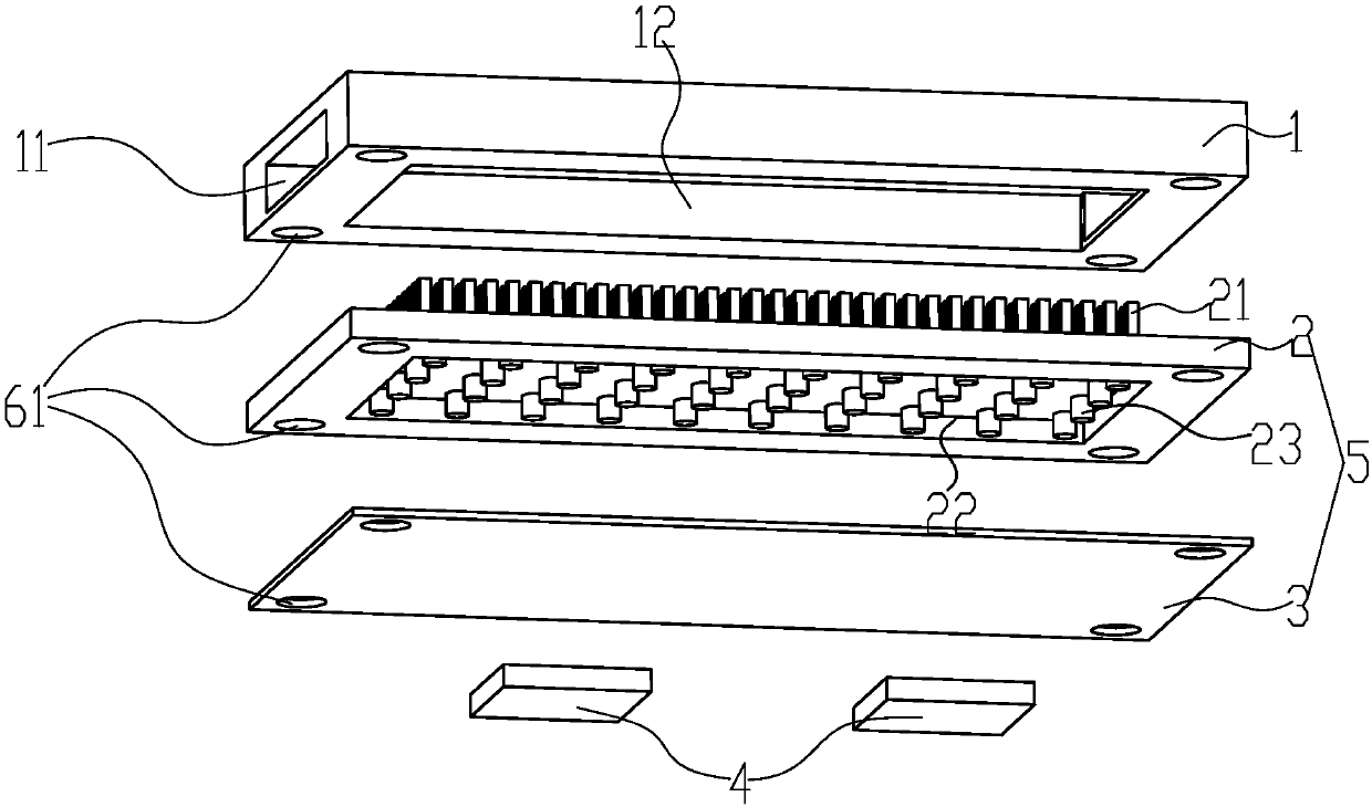
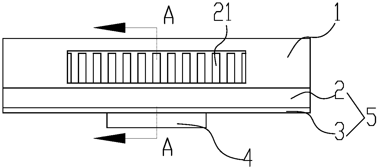
[0044] Such as Figure 1 to Figure 4 As shown, the integrated packaging structure of the IGBT chip and the phase change chamber includes the end cover 1, the upper shell plate 2, the bottom plate 3 and the IGBT chip 4 that are sequentially fixed together. The IGBT chip 4 is welded on the bottom surface of the bottom plate 3, and the upper The side of the shell plate 2 close to the end cover 1 is provided with several columnar fins 21, the end cover 1 and the upper shell plate 2 enclose a heat exchange space for heat exchange, and several columnar fins 21 are located in the heat exchange space, The heat exchange space is provided with at least one coolant inlet and outlet 11, and the upper shell plate 2 is provided with several support columns 23 on the side close to the bottom plate 3, and the upper shell plate 2 and the bottom plate 3 form a closed cavity of the chamber, and A support column 23 is loca...


PUM


Abstract

The invention relates to an integrated packaging structure of an IGBT chip and a phase-transformation soaking plate. The integrated packaging structure is composed of an end cover, an upper shell plate, a bottom plate and an IGBT chip that are connected fixedly and successively. The IGBT chip is welded to the bottom of the bottom plate. A plurality of columnar fins are arranged at one side, approaching the end cover, of the upper shell plate; heat-exhange space for heat exchanging is encircled by the end cover and the upper shell plate; and the plurality of columnar fins are arranged in the heat-exhange space with at least one cooling liquid inlet and outlet. A plurality of support posts are arranged at one side, approaching the bottom plate, of the upper shell plate; an enclosed soaking plate cavity is encircled by the upper shell plate and the bottom plate; the plurality of support posts are arranged in the enclosed soaking plate cavity; and the enclosed soaking plate cavity filled with a working medium is in a vacuum state. Compared with the prior art of setting a heat-conducting film or coating a thermal conductive paste between the IGBT chip and the bottom plate, the integrated packaging structure has the following beneficial effects: the IGBT chip is welded to the bottom plate of the soaking plate, so that the contact thermal resistance is reduced effectively; and a high-temperature process is carried out before a process of liquid injection, vacuumization, and sealing of the soaking plate, so that the soaking plate is protected from being damaged by thermal expansion.

Description

technical field [0001] The invention relates to the field of heat dissipation of electronic components, in particular to an integrated package structure of an IGBT chip and a phase-change vapor chamber and a manufacturing method thereof. Background technique [0002] With the continuous development of the electronic information industry, electronic products continue to develop towards the trend of thinner, smaller, and higher power. The power is getting higher and higher, and the volume is getting smaller and smaller. Then, how to better dissipate heat has become an urgent problem to be solved. . The local heat flux density of the chip is too high, and the heat is easy to accumulate in the center, resulting in excessive local temperature, hot spots and shortening the service life of electronic products, especially for high-power, high heat-flux IGBT (Insulated Gate Bipolar Transistor) chips. Pole transistor is a composite fully-controlled voltage-driven power semiconductor ...

Claims


Application Information

Patent Timeline
Patent Type & Authority Applications(China)
IPC IPC(8): H01L23/473H01L23/427H01L23/367H01L21/48
CPCH01L21/4882H01L23/367H01L23/4275H01L23/473
Inventor 黄光文李勇周文杰何柏林陈韩荫陈创新
Owner SOUTH CHINA UNIV OF TECH
Why Eureka
Try Eureka