Fabrication of nanostructured substrates comprising a plurality of nanostructure gradients on a single substrate

A nanostructure and substrate technology, applied in the direction of nanotechnology, nanotechnology, nanotechnology, etc. for information processing, can solve the problems of optical path realignment, complex replacement process, etc.

Active Publication Date: 2018-05-11
MAX PLANCK GESELLSCHAFT ZUR FOERDERUNG DER WISSENSCHAFTEN EV
View PDF16 Cites 7 Cited by
  • Summary
  • Abstract
  • Description
  • Claims
  • Application Information

AI Technical Summary

Problems solved by technology

This replacement process is very complex and can lead to various problems in terms of realignment of optical paths, sensor alignment, comparability between different filters, etc.

Method used


Image

  • Fabrication of nanostructured substrates comprising a plurality of nanostructure gradients on a single substrate
  • Fabrication of nanostructured substrates comprising a plurality of nanostructure gradients on a single substrate
  • Fabrication of nanostructured substrates comprising a plurality of nanostructure gradients on a single substrate

Examples


example 1

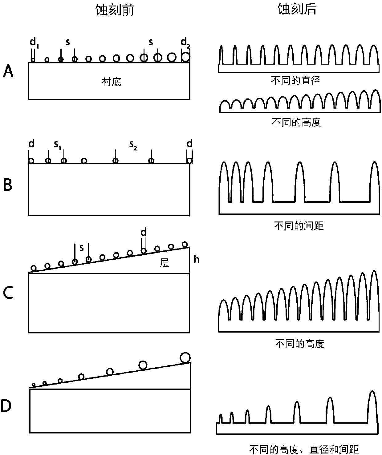
[0093] Formation of multiple nanostructure gradients on the same single substrate

[0094] 1. Provide composite substrate

[0095] Primary substrates, such as transparent quartz glass, are coated by sputtering (UHV systems; target 99.995% SiO 2 , 3.00 inches in diameter, 0.125 inches thick, using 2*10 with 150W RF power -3 O of mbar 2 and Ar room temperature sputtering, base pressure: 10 -6 mbar) is coated with at least one layer of a material easily etched by RIE, such as SiO 2 formed.

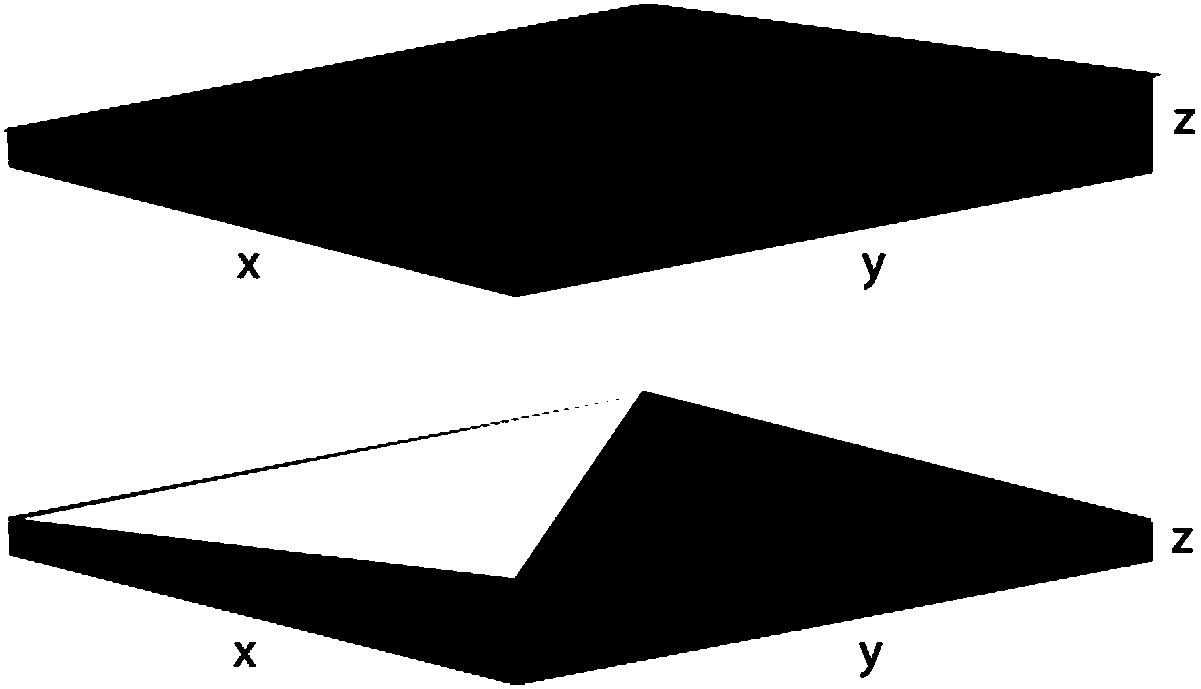
[0096] By slowly tilting the substrate during deposition, a gradient of thickness variation can be deposited on the substrate. By choosing an appropriate deposition method and varying the tilt orientation during deposition, simple 2D gradients or more complex 3D gradients with linearly or otherwise increasing layer thicknesses can be formed ( figure 2 comparison in ).

[0097] 2. Provide nanoparticle arrays on the substrate surface

[0098] The surface of the graded "sacrificial" la...

example 2

[0139] Characterization of nanostructured composite or primary substrates

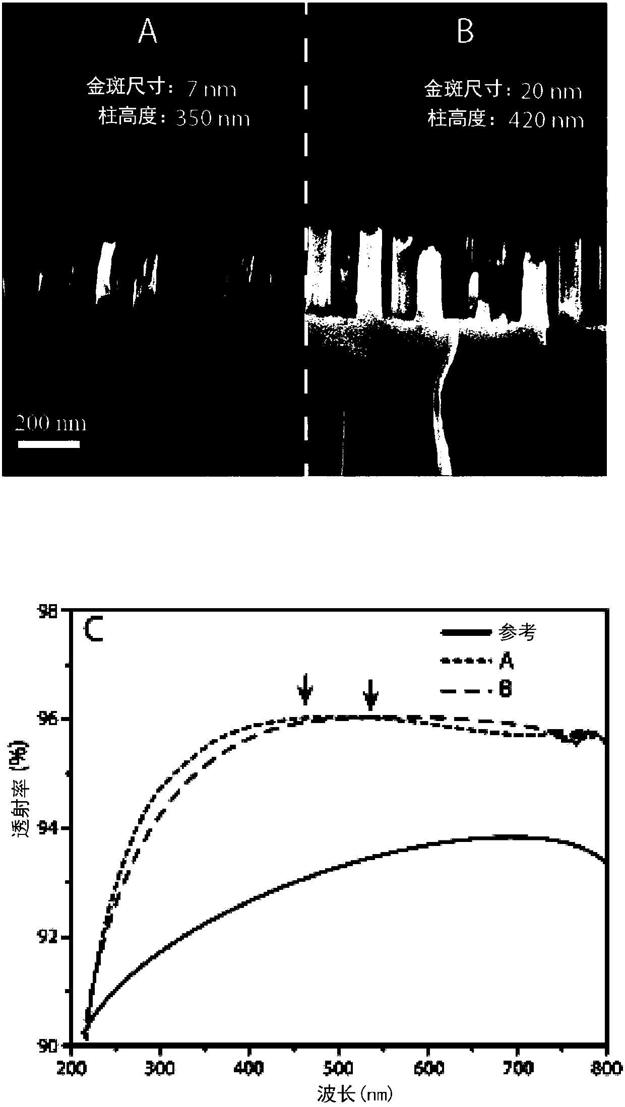
[0140] with gradient SiO 2 layer and electroless treated BCML patterned clear quartz samples were etched on one side using the RIE process as described above. The transmittance was then measured as a function of wavelength using a spectrometer device at ~1 mm beam size. The sample was split after measurement to take SEM pictures of the column cross-section. figure 1 A shows the geometry of the pillar structure on one side of the sample (~42 nm in diameter and 350 nm in height), figure 1 B shows the geometry on the opposite side of the same sample (~78 nm in diameter and 420 nm in height). figure 1 C shows the corresponding improved total transmission (compared to common transparent quartz substrates) and the shift in maximum projection.


PUM

PropertyMeasurementUnit
heightaaaaaaaaaa
thicknessaaaaaaaaaa
diameteraaaaaaaaaa

Abstract

The invention relates to a method for producing a nanostructured substrate comprising an array of protruding nanostructures, in particular nano-pilalrs, which method comprises at least the following steps: a) providing a primary substrate; b) depositing at least one layer of a material capable to be removed by means of reactive ion etching (RIE) onto said primary substrate which layer comprises apredetermined gradient of its thickness; c) depositing a nanostructured etching mask onto the graded layer deposited in step b); d) generating protruding structures, in particular nanopillars, in thegraded layer deposited in step b) by means of reactive ion etching (RIE), wherein simultaneously at least 2, preferably 3, predetermined continuous gradients of geometric parameters of the protrudingstructures are generated on the same substrate- More specifically, the geometric parameters are selected from the group comprising the height, diameter and spacing - of the protruding nanostructures.A further aspect of the invention relates to a nanostructured substrate comprising an array of protruding nanostructures obtainable by the method as outlined above. In a preferred embodiment of said nanostructured substrate, each of the protruding nanostructures simultaneously represents an element of 3 continuous gradients of the height, diameter and spacing of said protruding nanostructures.

Description

technical field [0001] Various methods are known in the prior art for forming nanostructures on various substrate surfaces, for example by means of electron beam lithography or various etching techniques. Such nanostructures can be used, for example, to immobilize target groups, such as biomolecules, or to provide antireflective coatings on corresponding substrates. Background technique [0002] In general, antireflective coatings are made of several types of thin layers. However, these antireflection layers are only effective in a limited wavelength range, usually only allow slight variations in the angle of incidence and are very difficult to adjust to the required projection or reflection specifications. Moth-eye-like nanostructures (MOES) exhibit a combination of high transmittance nearly independent of wavelength with very low reflectivity and could solve many of these problems (Morhard, C., Nanolithographie, 1-149 (2010); Brunner et al., Applied Optics 52, 4370-4376 ...

Claims


Application Information

Patent Timeline
Patent Type & Authority Applications(China)
IPC IPC(8): B81C1/00B82Y10/00B82Y40/00G02B1/118H01L21/3065H01L21/308
CPCB82Y10/00B82Y40/00G02B1/118B81B2203/0361G02B2207/101H01L31/00B81C1/00031
Inventor Z·刁J-H·迪克斯J·P·施帕茨
Owner MAX PLANCK GESELLSCHAFT ZUR FOERDERUNG DER WISSENSCHAFTEN EV
Why Eureka
Try Eureka