
Device for regulating and controlling thin film material growth through substrate electrification

A thin-film material and substrate technology, which is applied in the field of devices for regulating the growth of thin-film materials, can solve the problems of limited ability to control the structure of two-dimensional materials, incapable of substrate adsorption performance, electronic energy state and catalytic activity regulation, etc.

Inactive Publication Date: 2018-05-25
PEKING UNIV
View PDF7 Cites 1 Cited by
  • Summary
  • Abstract
  • Description
  • Claims
  • Application Information

AI Technical Summary

Problems solved by technology

It cannot control the adsorption performance, electronic energy state and catalytic activity of the substrate.
Therefore, the ability to control the structure of two-dimensional materials is very limited.

Method used


Image

  • Device for regulating and controlling thin film material growth through substrate electrification
  • Device for regulating and controlling thin film material growth through substrate electrification
  • Device for regulating and controlling thin film material growth through substrate electrification

Examples


Embodiment 1

[0057] Embodiment 1, the process of power-on device and preparation thin film material on metal substrate

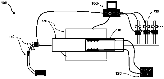
[0058] In this example, the controllable preparation device of two-dimensional thin film materials such as figure 1 As shown, the apparatus 100 includes a CVD reaction chamber 110 , a substrate power supply system 120 , a reaction gas management system 130 , an exhaust management system 140 , a heating system 150 and a central control system 160 .

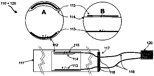
[0059] In order to facilitate placing the substrate, connecting the circuit, and quickly pulling the temperature up and down, a CVD reaction chamber 110 with an inner and outer sleeve structure is used in this embodiment. Such as figure 2 As shown, 111 and 112 are respectively a large quartz tube and a quartz casing, both of which are made of quartz. The large quartz tube 111 has an outer diameter of 50 mm, an inner diameter of 44 mm, and a length of 1800 mm; the outer diameter of the quartz sleeve 112 is 42 mm, an inner di...

Embodiment 2

[0063] Embodiment 2, the process of applying power to the insulating substrate and preparing the thin film material

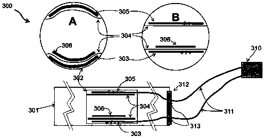
[0064] In this embodiment, the reaction chamber and substrate power supply system in the controllable preparation device of two-dimensional thin film materials are as follows: image 3 shown. Other parts of the device such as CVD reaction chamber, reaction substrate power supply system, reaction gas management system, exhaust management system, heating system and central control system, etc. figure 1 shown.

[0065] In order to facilitate the placement of the substrate, connection of the circuit, and rapid heating and cooling, the CVD reaction chamber 300 with an inner and outer sleeve structure is used in this embodiment. Such as image 3 As shown, 301 and 302 are respectively a large quartz tube and a quartz casing, both of which are made of quartz. The large quartz tube 301 has an outer diameter of 50 mm, an inner diameter of 44 mm, and a length of 1800 m...


PUM


Abstract

The invention discloses a device for regulating and controlling the thin film material growth through substrate electrification. The device is characterized in that on the basis of the existing CVD (chemical vapor deposition) reaction device, a substrate electrification system is added; the substrate electrification system comprises a conducting circuit, a metal pole plate, a plug and a power supply; the metal pole plate is positioned in a CVD reaction cavity; the plug and the power supply are positioned outside the CVD reaction cavity; the metal pole plate is connected with the plug and the power supply through the conducting circuit. By using the device, positive and negative static charges or current can be exerted on the conducting substrate; an insulation substrate is polarized, so that electrostatic charges can be controllably generated at the surface; the goal of regulating and controlling the electric potential, the adsorbability, the electron energy state and the catalytic activity of the freely grown substrate is achieved. By using device and the growth method, the monocrystal size, the uniformity, the doping concentration, the layer number, the interlayer stacking mode,the twist angle, the chirality, the cleanliness and the like can be conveniently controlled in the thin film material preparation process.

Description

technical field [0001] The invention relates to a device for regulating and controlling the growth of a thin film material by applying electricity to a substrate. Background technique [0002] Two-dimensional materials have many unique properties due to the quantum confinement effect in the thickness direction, so there are many promising applications. Typical two-dimensional materials include graphene, hexagonal boron nitride, molybdenum disulfide, etc., and they are only one or a few atomic layers thick in the thickness direction. [0003] It is very important to control the single crystal size, doping concentration, layer number, interlayer stacking mode and twist angle, chirality, cleanliness, etc. of two-dimensional thin film materials, because these aspects directly affect its electrical, optical and The chemical properties thus determine its application in various aspects. [0004] Chemical vapor deposition (CVD) stands out among various preparation technologies and...

Claims


Application Information

Patent Timeline
Patent Type & Authority Applications(China)
IPC IPC(8): C30B25/00C30B29/60
CPCC30B25/00C30B29/60
Inventor 刘忠范孙禄钊张金灿林立彭海琳
Owner PEKING UNIV
Learn More