High temperature resistance switching power source based on gallium nitride device and DSP chip and working method thereof
A technology of switching power supply and working method, which is applied in the direction of high-efficiency power electronic conversion, instruments, electrical components, etc., and can solve the problem that there is no method or device to improve the switching power supply circuit to cope with the high temperature underground working environment, the selection range is limited, and the switching power supply circuit cannot be solved. high temperature issues
- Summary
- Abstract
- Description
- Claims
- Application Information
AI Technical Summary
Problems solved by technology
Method used
Image
Examples
Embodiment 1
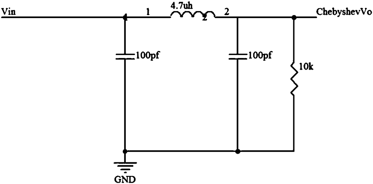
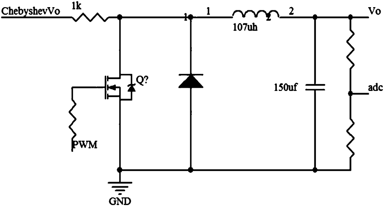
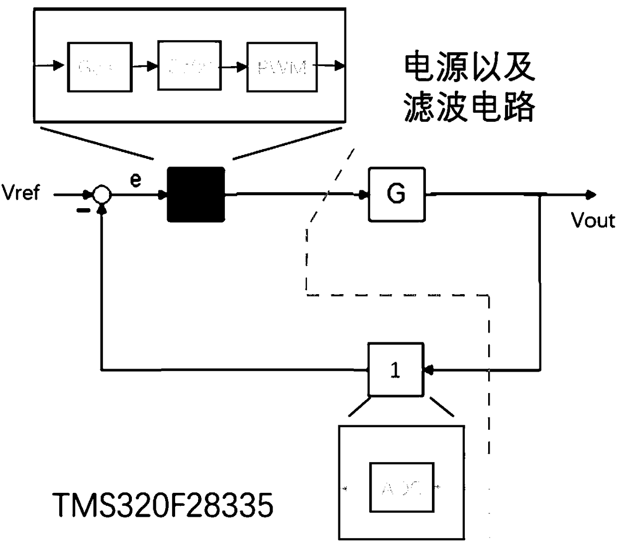
[0040] Such as Figure 1-3 Shown.
[0041] A high temperature resistant switching power supply based on gallium nitride devices and DSP chips, including Chebyshev II input anti-aliasing filter circuit, GaN transistor, switching power supply buck circuit, and DSP chip;
[0042] The Chebyshev II input anti-aliasing filter circuit is connected to the drain of the GaN transistor; the drain of the GaN transistor is connected to the adc pin of the DSP chip through the switching power supply buck circuit; the pwm output pin of the DSP chip is connected to the gate of the GaN transistor The pole is connected to realize the control of the switching time of the GaN transistor; the DSP chip, the GaN transistor and the switching power supply buck circuit form a closed-loop control system.
[0043] Chebyshev II input anti-aliasing filter circuit filters out the high frequency part of the input signal, so that the signal input to the adc pin meets the sampling theorem. In terms of the frequency r...
Embodiment 2
[0050] Such as Figure 4-6 Shown.
[0051] A working method of the switching power supply circuit as described in embodiment 1, including the following steps:
[0052] 1) Input signal input Chebyshev type II input anti-aliasing filter circuit, Chebyshev type II input anti-aliasing filter circuit filters out the high frequency part of the input signal, so that the signal input to the adc pin meets the sampling theorem;
[0053] 2) The input signal is input to the GaN transistor through the drain of the GaN transistor after passing the Chebyshev II input anti-aliasing filter circuit;
[0054] 3) The pwm output signal triggers the interrupt of the adc pin;
[0055] 3.1) When an interrupt comes, the instruction register IR inside the DSP chip is filled with a new value, and the program in the DSP chip jumps out of the main function and executes the adc interrupt function;
[0056] 3.2) The adc interrupt function performs digital-to-analog conversion on the output signal of the buck circuit t...
Embodiment 3
[0067] As for the working method of the switching power supply circuit described in embodiment 2, further, in the step 3.4), the design method of the control algorithm function is to obtain the buck circuit transfer function in the s domain through the Laplace transform of the buck circuit, Realize the preliminary modeling of the closed-loop system; with the help of matlab, add moving zeros and poles on the basis of the existing Bode diagram to obtain the control function; the control function is transformed into the time domain through inverse Laplace transform, and finally The z transformation is the control algorithm function.
PUM
 Abstract
Description
Claims
Application Information


