
Preparation method of sandwich type photoresist sacrificial layer

A photoresist, sandwich-type technology, applied in coating, manufacturing microstructure devices, metal material coating process, etc., can solve the problems of difficult to achieve high-precision pattern preparation, high equipment requirements, difficult step structure, etc. The effect of low dependence, low heat treatment temperature, and simple preparation

Active Publication Date: 2018-06-01
NO 54 INST OF CHINA ELECTRONICS SCI & TECH GRP
View PDF6 Cites 4 Cited by
  • Summary
  • Abstract
  • Description
  • Claims
  • Application Information

AI Technical Summary

Problems solved by technology

[0003] Among them, the positive photoresist (hereinafter referred to as the positive photoresist) has the advantages of high resolution, easy processing of graphics, small stress, good leveling, and easy release. However, due to its own characteristics, the positive photoresist also has certain limitations: It is difficult to accurately realize the step structure of the sacrificial layer of positive resist, such as the precise preparation of structures such as bumps; the problem of sol is common when the positive resist is evenly distributed on the patterned positive resist; the double-layer photoresist sacrificial layer needs to select a specific Negative photoresist is used as the bottom layer, it is difficult to achieve high-precision pattern preparation, and it must be released by dry method, which requires high equipment

Method used


Image

  • Preparation method of sandwich type photoresist sacrificial layer
  • Preparation method of sandwich type photoresist sacrificial layer
  • Preparation method of sandwich type photoresist sacrificial layer

Examples


Embodiment Construction

[0029] Below in conjunction with specific embodiment and attached Figure 1-6 The present invention is further explained.

[0030] figure 1 It is a schematic diagram of a RFMEMS switch with contacts, including the lower circuit structure and the suspension structure, and there is a bump structure in the suspension structure; to form such figure 1 Suspension structure shown in, the present invention has designed a kind of preparation method of sandwich type photoresist sacrificial layer, comprises the following steps:

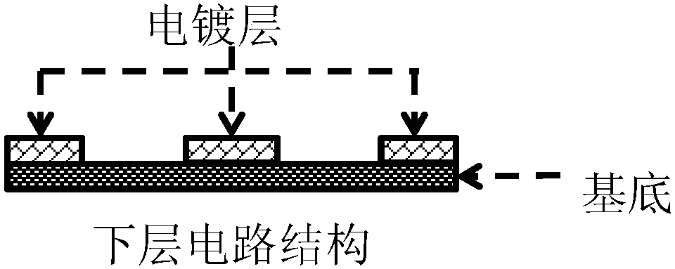
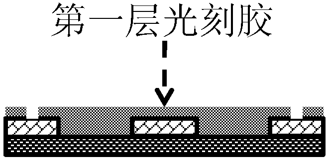
[0031] 1. Preparation of lower positive glue: figure 2 It is a schematic diagram of the lower circuit before making the sacrificial layer. The lower circuit structure includes the substrate and the circuit structure processed by electroplating; the first layer of positive resist is spin-coated on the lower circuit, and the patterning is completed by exposure and development. After patterning, the photoresist of this layer is heat-treated to form such as im...


PUM


Abstract

The invention discloses a preparation method of a sandwich type photoresist sacrificial layer in the field of manufacturing of RF MEMS devices. The preparation method mainly comprises the following five steps: preparation of lower layer photoresist, growth of a barrier layer, preparation of upper layer photoresist, etching of a Cu layer and heat treatment. According to the method, the problem of mutual dissolution between the two layers of photoresist is avoided by importing a Cu barrier layer, and the prepared sacrificial layer has the characteristics of simple release, accurate salient pointheight control, low device dependency, capability of manufacturing complex patterns, etc.

Description

technical field [0001] The invention relates to the field of RFMEMS device manufacturing, in particular to a method for preparing a photoresist sacrificial layer of an RFMEMS device. technical background [0002] RFMEMS devices have the advantages of small size, low power consumption, high isolation, and low loss, and have broad application prospects in the fields of communication, aerospace, and biomedicine. In MEMS manufacturing, sacrificial layer technology is often used, that is, a filling layer is grown on the lower circuit, and the upper circuit is processed on the filling layer, and finally this part of the filling layer is etched away by means of chemical etching to obtain a suspended upper layer. structure. Since the removed filling layer only acts as a separation layer, it is called a sacrificial layer. Existing sacrificial layer materials include Si, SiO2, PI, photoresist, Al, Ti and other materials. [0003] Among them, the positive photoresist (hereinafter re...

Claims


Application Information

Patent Timeline
Patent Type & Authority Applications(China)
IPC IPC(8): B81C1/00
CPCB81C1/00349B81C1/00388
Inventor 陈雨党元兰刘晓兰庄治学梁广华徐亚新
Owner NO 54 INST OF CHINA ELECTRONICS SCI & TECH GRP
Learn More