Red light semiconductor laser structure with aluminum-free waveguide layer

A waveguide layer and semiconductor technology, applied in the direction of semiconductor lasers, lasers, laser components, etc., can solve problems such as easy to form defects, high material growth requirements, and affect laser performance, so as to reduce the formation of cavity surface defects and light absorption , Improve the effect of anti-burning ability

Active Publication Date: 2018-06-29
Shandong Huaguang Optoelectronics Co. Ltd.
View PDF6 Cites 7 Cited by
  • Summary
  • Abstract
  • Description
  • Claims
  • Application Information

AI Technical Summary

Problems solved by technology

[0007] Aiming at the disadvantages that the waveguide layer of the existing red light semiconductor laser is made of aluminum-containing material, which requires high material growth, and is easy...

Method used


Image

  • Red light semiconductor laser structure with aluminum-free waveguide layer

Examples


Embodiment 1

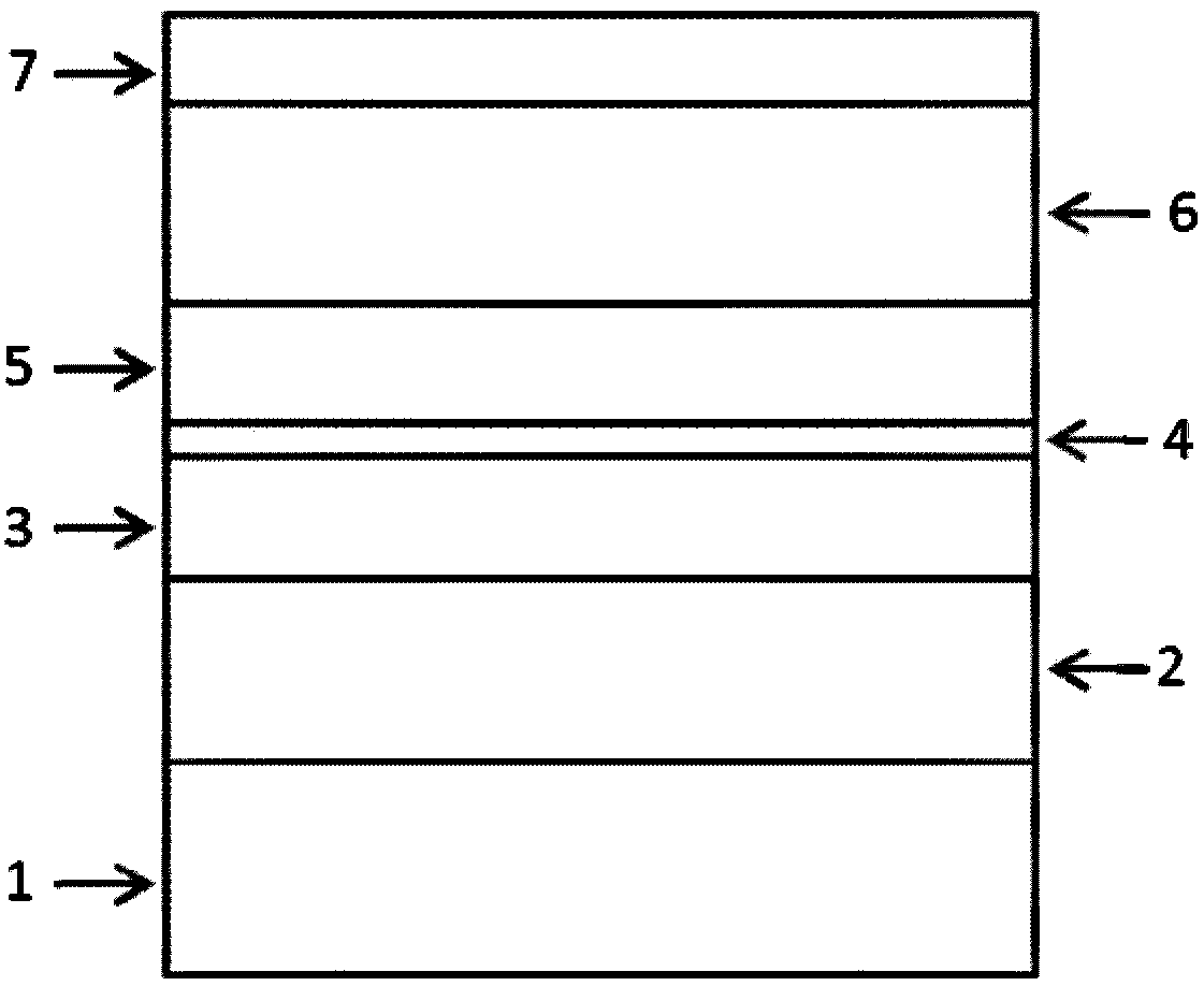
[0034] A red semiconductor laser structure without an aluminum waveguide layer, such as figure 1 As shown, it includes a substrate 1 , a lower confinement layer 2 , a lower waveguide layer 3 , a quantum well layer 4 , an upper waveguide layer 5 , an upper confinement layer 6 and an ohmic contact layer 7 from bottom to top.

[0035] The substrate 1 is an N-type GaAs (100) single crystal substrate with a orientation of 10°.

[0036] The lower confinement layer 2 is N-type (Al 0.6 Ga 0.4 ) 0.5 In 0.5 P.

[0037] The lower waveguide layer 3 is Ga with a thickness of 100nm 0.5 In 0.5 P, grown at 700°C, is a disordered structure with a band gap of 1.91eV.

[0038] The quantum well layer 4 is Ga with a thickness of 6nm 0.5 In 0.5 P, grown at a temperature of 600°C, is an ordered structure with a band gap of 1.84eV and a red light with a laser wavelength of about 660nm.

[0039] The upper waveguide layer 5 is Ga with a thickness of 100nm 0.5 In 0.5 P, grown at 700°C, is a...

Embodiment 2

[0043] According to the structure of a red light semiconductor laser without an aluminum waveguide layer described in Embodiment 1, the difference is that,

[0044] The substrate 1 is an N-type GaAs (100) single crystal substrate with a orientation of 12°.

[0045] The lower confinement layer 2 is N-type (Al 0.5 Ga 0.5 ) 0.5 In 0.5 P.

[0046] The lower waveguide layer 3 is Ga with a thickness of 100nm 0.5 In 0.5 P, grown at 680°C, is a disordered structure with a band gap of 1.91eV.

[0047] The quantum well layer 4 is Ga with a thickness of 6nm 0.45 In 0.55 P, with a growth temperature of 620°C, is an ordered structure with a band gap of 1.79eV and a red light with a laser wavelength of about 680nm.

[0048] The upper waveguide layer 5 is Ga with a thickness of 100nm 0.5 In 0.5 P, grown at 680°C, is a disordered structure with a band gap of 1.91eV.

[0049] The upper confinement layer 6 is a P-type (Al 0.5 Ga 0.5 ) 0.5 In 0.5 P.

[0050] The ohmic contact l...


PUM

PropertyMeasurementUnit
Bandgapaaaaaaaaaa
Bandgapaaaaaaaaaa
Thicknessaaaaaaaaaa

Abstract

The invention relates to a red light semiconductor laser structure with an aluminum-free waveguide layer, which sequentially comprises a substrate, a lower limit layer, a lower waveguide layer, a quantum well layer, an upper waveguide layer, an upper limit layer and an ohmic contact layer from the bottom up, wherein the lower waveguide layer, the quantum well layer and the upper waveguide layer are made of a gallium indium phosphide material. The waveguide layer adopts the aluminum-free gallium indium phosphide material, so that there is no aluminum in an active region, and requirements for the growth environment, especially for the concentration of oxygen impurities, are no longer so harsh. Meanwhile, the oxidation resistance is increased because there is no aluminum in the active regionwhen cavity surface cleavage is performed, so that cavity surface defects are effectively reduced. The design not only reduces oxygen impurity defects inside the material, but also reduces the formation of cavity surface defects, thereby being capable of reducing the light absorption, and improving the anti-burning ability of the cavity surface and the life of a semiconductor laser.

Description

technical field [0001] The invention relates to a red light semiconductor laser structure without an aluminum waveguide layer, belonging to the technical field of semiconductor lasers. Background technique [0002] The red light semiconductor laser has the advantages of small size, long life and high photoelectric conversion efficiency. It is gradually replacing the traditional He-Ne gas laser and ruby ​​solid-state laser, and is widely used in optical storage systems, barcode readers, and industrial alignment and marking instruments. , healthcare equipment, etc. In addition, it is also a red light source for laser display devices such as laser TVs and portable projectors. These applications require the laser to maintain a stable optical mode and laser power output, and have high requirements on the life and reliability of the laser. [0003] The earliest red light semiconductor lasers used AlGaAs material systems, such as 780nm AlGaAs semiconductor lasers for CD players. ...

Claims


Application Information

Patent Timeline
IPC IPC(8): H01S5/323H01S5/34
CPCH01S5/323H01S5/34
Inventor 朱振张新徐现刚
Owner Shandong Huaguang Optoelectronics Co. Ltd.
Why Eureka
Try Eureka