High-efficiency energy-saving LED preparation technology

A preparation process, high-efficiency and energy-saving technology, applied in the field of lighting, can solve the problems of commercial production, high preparation cost, complicated process, etc., and achieve reduction of production cost and process complexity, easy controllable wavelength, and indium component content stable effect

Inactive Publication Date: 2018-07-06
李丹丹
View PDF5 Cites 4 Cited by
  • Summary
  • Abstract
  • Description
  • Claims
  • Application Information

AI Technical Summary

Problems solved by technology

However, at the present stage, the preparation cost of graphene thin film layer is high and the process is complicated, and commercial production cannot be realized. At the same time, the installation of graphene thin film layer is easy to cause other problems such as carbon contamination. It is necessary to seek other alternative means to improve LED luminous efficiency.

Method used


Image

  • High-efficiency energy-saving LED preparation technology
  • High-efficiency energy-saving LED preparation technology
  • High-efficiency energy-saving LED preparation technology

Examples


Embodiment 1

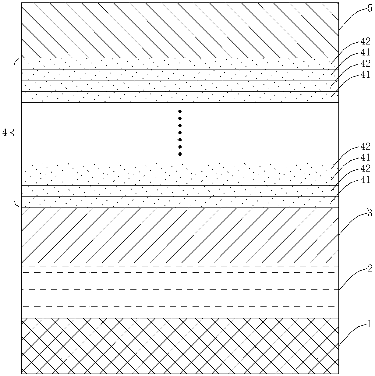
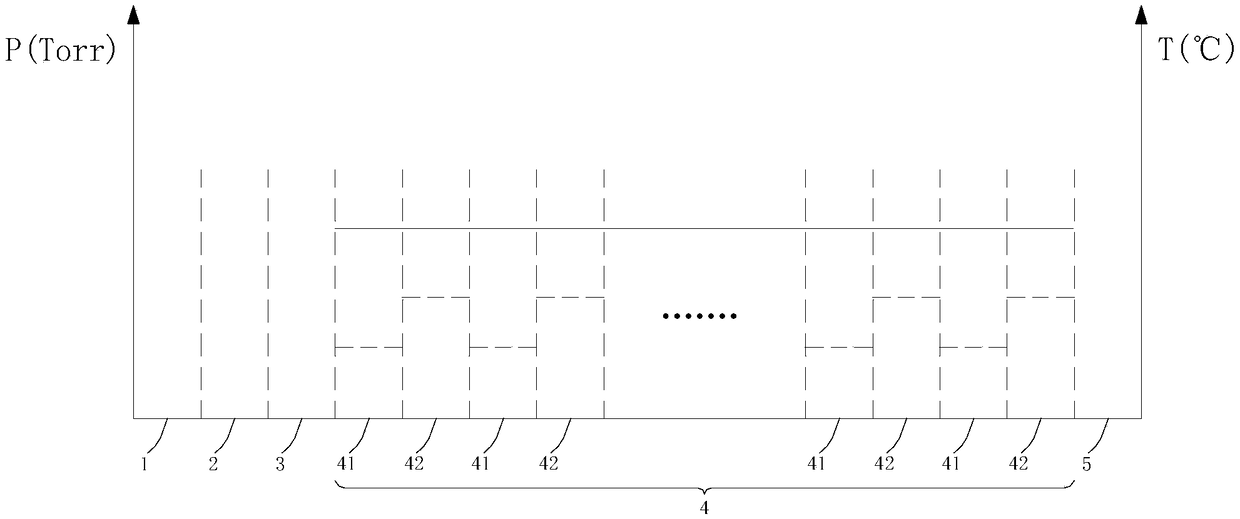
[0027] In the prior art, LED structures such as figure 1 As shown, it includes a buffer layer 2, an N-type GaN layer 3, a light-emitting layer 4, and a P-type GaN layer 5 sequentially deposited on a substrate 1 by a metal-organic chemical vapor deposition process; the light-emitting layer 4 includes periodically stacked quantum well layers 41 and quantum barrier layer 42, the pressure and temperature when forming quantum well layer 41 and quantum barrier layer 42 are as figure 2 As shown (the horizontal solid line above the coordinate system in the figure represents the pressure, and the horizontal dotted line below represents the temperature, and the expressions in the subsequent corresponding figures are consistent and will not be repeated), in the prior art, when forming the quantum well layer 41 and the quantum well layer 41 The pressure of the barrier layer 42 is equal, and the temperature for forming the quantum well layer 41 is lower than the temperature for forming th...


PUM


Abstract

The invention provides a high-efficiency energy-saving LED preparation technology. A buffer layer, an N type GaN layer, a luminescent layer and a P type GaN layer successively deposed on a substrate in a vapor deposition technology of metal organic chemistry are included; and the luminescent layer comprises quantum well and barrier layers stacked periodically, at least one quantum well layer is ahigh-pressure quantum well layer, at least one quantum barrier layer is a low-pressure quantum barrier layer, and the pressure formed in the high-pressure quantum well layer is higher than that formedin the low-pressure quantum barrier layer. Indium is doped into gallium nitride via high pressure, the doping amount of indium is not improved by reducing the growth temperature, the quantum well layers can be deposed at a higher temperature, and the crystallization quality of the obtained quantum well layers is higher; and the cost is low, and realization is easy.

Description

technical field [0001] The invention relates to the technical field of lighting, in particular to a high-efficiency and energy-saving LED preparation process. Background technique [0002] LED (LightingEmittingDiode) lighting is light-emitting diode lighting, which is a semiconductor solid-state light-emitting device. It uses a solid semiconductor chip as a light-emitting material. In the semiconductor, the excess energy is released through the recombination of carriers to cause photon emission, and directly emits red, yellow, blue, and green light. On this basis, using the principle of three primary colors, Adding fluorescent powder can emit light of any color. The lighting fixtures manufactured using LEDs as light sources are LED lamps. [0003] The LED manufacturing process is divided into epitaxy, chip front-end, chip back-end, packaging and other links. Epitaxy deposits a buffer layer, an N-type GaN layer, a light-emitting layer, and a P-type GaN layer on a sapphire s...

Claims


Application Information

Patent Timeline
Patent Type & Authority Applications(China)
IPC IPC(8): H01L33/00H01L33/06H01L33/32
CPCH01L33/007H01L33/0075H01L33/06H01L33/32
Inventor 李丹丹
Owner 李丹丹
Why Eureka
Try Eureka