A Photolithographic Process Method for Realizing High Steepness and Deep Silicon Etching Structure

A technology of deep silicon etching and photolithography, which is applied in the manufacture of electrical components, circuits, semiconductors/solid-state devices, etc., can solve the problems affecting the quality of deep silicon etching structures, structure morphology, poor line width compliance, and increase the process Complexity and other issues, to achieve the effect of improving etching resistance and pattern compliance, strong etching resistance, and improving compactness

Active Publication Date: 2020-04-10
BEIJING INST OF AEROSPACE CONTROL DEVICES
View PDF3 Cites 0 Cited by
  • Summary
  • Abstract
  • Description
  • Claims
  • Application Information

AI Technical Summary

Problems solved by technology

However, thicker photoresist mask patterns have problems such as structural morphology and line width compliance, which directly affect the quality of deep silicon etching structures.
When a composite mask of photoresist and dielectric layer is used, a thin layer of photoresist can be used, but the preparation and removal of the dielectric layer mask significantly increases the complexity of the process

Method used


Image

  • A Photolithographic Process Method for Realizing High Steepness and Deep Silicon Etching Structure
  • A Photolithographic Process Method for Realizing High Steepness and Deep Silicon Etching Structure

Examples


Embodiment Construction

[0024] Below in conjunction with accompanying drawing and specific embodiment the present invention is described in further detail:

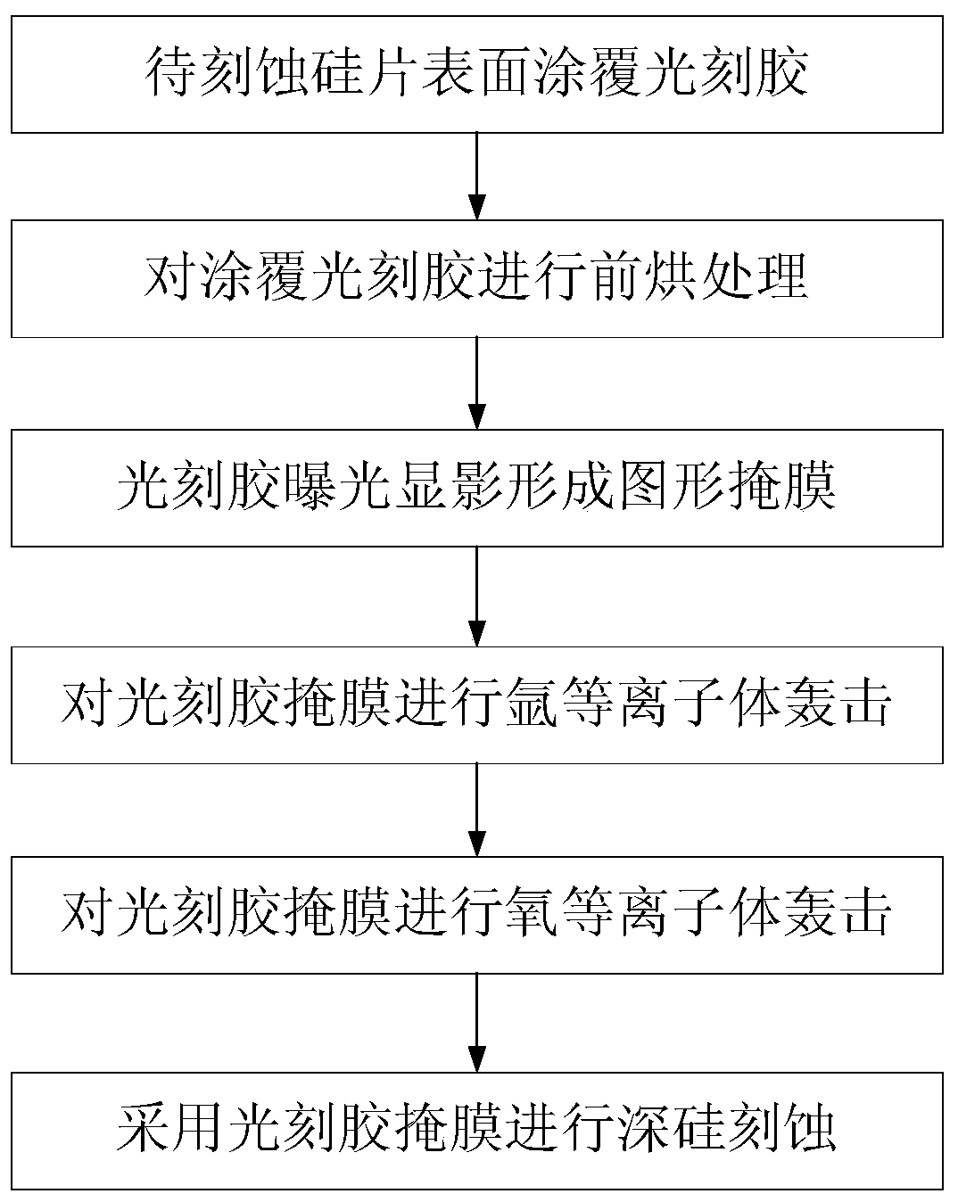
[0025] Such as figure 1 Shown is the flow chart of photolithography process method step, by figure 1 It can be seen that a photolithography process method for realizing a high-steep deep silicon etching structure includes the following steps:

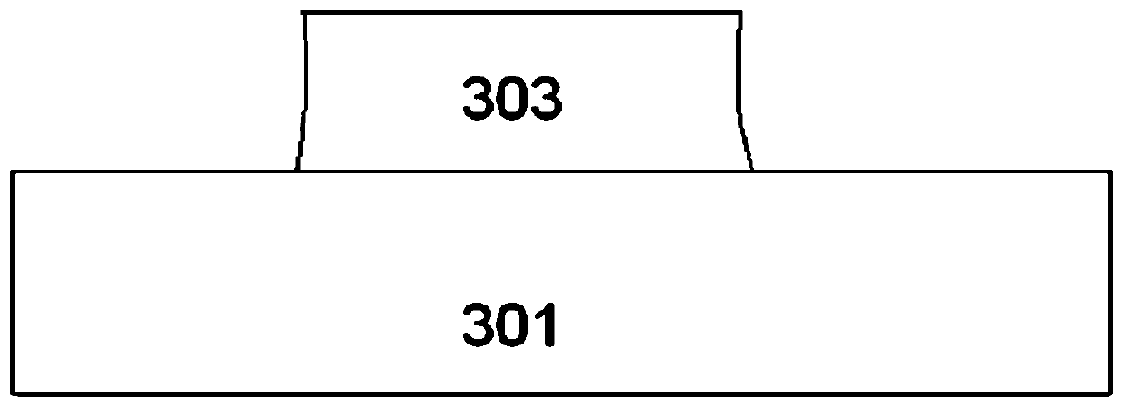
[0026] Step (1), cleaning and drying the wafer 301 to be etched, placing the wafer 301 to be etched horizontally in hot nitrogen, the temperature of the hot nitrogen is 85-105°C; The upper surface of the etched wafer 301 is coated with a photoresist 303; the thickness of the coated photoresist 303 is 2-5 μm.

[0027] Step (2), using a hot plate to bake the wafer 301 coated with photoresist 303; the hot plate is fixedly arranged on the lower surface of the wafer 301; the hot plate bakes the bottom of the wafer 301; baking The temperature is 105-125°C; the baking time is 5-10min.

[0028] Step (3), afte...


PUM

PropertyMeasurementUnit
thicknessaaaaaaaaaa

Abstract

The invention discloses a photoetching technique for realizing high-steepness deep silicon etching structure and relates to the technical field of silicon micromachining. The photoetching technique includes following steps: step 1, coating the upper surface of a to-be-etched wafer with photoresist; step 2, adopting a hot plate to roast the wafer coated with the photoresist; step 3, performing exposure development on the upper surface of the photoresist to form a photoresist mark with predesigned graph; step 4, adopting argon plasma to bombard the outer surface of the photoresist mask; step 5,adopting oxygen plasma to remove edges and corners of the photoresist mask on the upper surface of the same to obtain a photoresist mask formed with final graph; step 6, performing deep silicon etching on the to-be-etched wafer through the photoresist mask formed with the final graph. The photoetching technique enables the photoresist mask to be higher in etching resistance and graph conformity and is conducive to realizing high-steepness deep silicon etching.

Description

technical field [0001] The invention relates to the technical field of silicon micromachining, in particular to a photolithography process method for realizing a high-steep deep silicon etching structure. Background technique [0002] Deep silicon etching process is one of the key processes in silicon micromachining. Sidewall steepness is an important indicator that is mainly concerned with deep silicon etching structures. It is well known that the etching mask is the primary factor affecting the morphology of etched deep silicon structures. There are two main types of etching masks commonly used in deep silicon etching processes. The first type uses a photoresist pattern with a certain thickness as a mask, and the second type uses a composite pattern of a thin layer of photoresist and a dielectric layer as a mask. mask. When a single-layer photoresist mask is used, the photoresist layer is required to have sufficient thickness to prevent the too thin resist mask from bei...

Claims


Application Information

Patent Timeline
Patent Type & Authority Patents(China)
IPC IPC(8): H01L21/027
CPCH01L21/027
Inventor 李新坤庄海涵梁德春刘福民吴浩越王风娇徐宇新
Owner BEIJING INST OF AEROSPACE CONTROL DEVICES
Why Eureka
Try Eureka