Quantum dot structure photoelectric detector and preparation method thereof

A technology of photodetectors and quantum dots, applied in the field of photodetectors, can solve problems such as large dark current and slow response speed, and achieve the effects of increasing life, improving device performance, and expanding the control range

Active Publication Date: 2018-07-13
UNIV OF ELECTRONICS SCI & TECH OF CHINA
View PDF3 Cites 19 Cited by
  • Summary
  • Abstract
  • Description
  • Claims
  • Application Information

AI Technical Summary

Problems solved by technology

The photodetector has a 7x10 13 The specific detection sensitivity of J, and the switch and device responsivity are high, but there are disadvantages of large dark current and slow response speed

Method used


Image

  • Quantum dot structure photoelectric detector and preparation method thereof
  • Quantum dot structure photoelectric detector and preparation method thereof
  • Quantum dot structure photoelectric detector and preparation method thereof

Examples


Embodiment Construction

[0020] In order to make the purpose, technical solution and advantages of the present application clearer, the present application will be further described in detail below in conjunction with the accompanying drawings and specific embodiments. For simplicity, some technical features known to those skilled in the art are omitted from the following description.

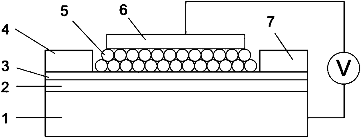
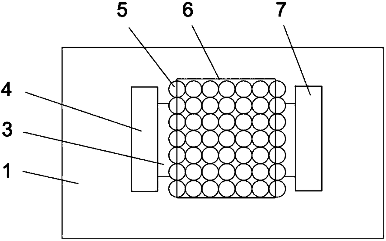
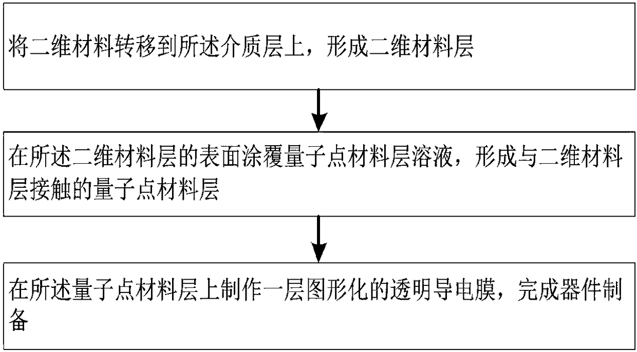
[0021] Such as image 3 As shown, the present embodiment provides a method for preparing a photodetector with a quantum dot structure, which is characterized in that it has a highly doped silicon substrate 1 covered with an aluminum oxide dielectric layer 2, comprising the following steps:

[0022] Using detergent, acetone, ethanol and deionized water to ultrasonically clean the highly doped silicon substrate 1 in sequence;

[0023] Transferring the graphene onto the alumina dielectric layer 2 to form a graphene layer 3;

[0024] Spin-coat photoresist on the graphene layer 3, photoresist off the photoresist at the po...


PUM


Abstract

The invention relates to the technical field of photoelectric detectors, in particular to a preparation method of a quantum dot structure photoelectric detector with a highly-doped substrate covered with a dielectric layer. The method includes steps: forming a two-dimensional material layer on the dielectric layer; coating the surface of the two-dimensional material layer with quantum dot materiallayer solution to form a quantum dot material layer; making a graphical transparent conductive film on the quantum dot material layer to complete preparation of the detector. The voltage assisted quantum dot structure photoelectric detector comprises the highly-doped substrate, the dielectric layer, the two-dimensional material layer, the quantum dot material layer and the transparent conductivefilm sequentially from bottom to top. A source electrode and a drain electrode are formed on the two-dimensional material layer which contacts with the quantum dot material layer to form a built-in electric field, and an adjustable modulation voltage identical to the built-in electric field in direction is applied between the transparent conductive film and the highly-doped substrate. Response speed and photoelectric current gain of the detector can be increased, and performances of the detector are remarkably improved.

Description

technical field [0001] The invention belongs to the technical field of photodetectors, and in particular relates to a voltage-assisted quantum dot structure photodetector. Background technique [0002] Graphene and graphene-like two-dimensional (2D) materials have attracted extensive attention due to their extraordinary electronic and optical properties, which hold great potential for optoelectronic applications such as photodetection. Although the research on graphene and graphene-like two-dimensional materials has made great progress, fundamental and practical problems still hinder the application of graphene and graphene-like two-dimensional materials. [0003] Graphene is a monoatomic layered two-dimensional material in which carbon atoms are arranged in a hexagonal honeycomb lattice and has many attractive electronic, optical, mechanical and thermal properties. The electrons transported in graphene behave as massless Dirac fermions, and there is a linear relationship b...

Claims


Application Information

Patent Timeline
Patent Type & Authority Applications(China)
IPC IPC(8): H01L51/48H01L51/46H01L51/42
CPCH10K71/12H10K30/30H10K30/354H10K30/65H10K2102/00Y02E10/549
Inventor 王军韩嘉悦杨明黄泽华苟君
Owner UNIV OF ELECTRONICS SCI & TECH OF CHINA
Why Eureka
Try Eureka