Method for welding circuit board

A welding method and circuit board technology, which is applied to printed circuits, printed circuit manufacturing, printed circuit assembly of electrical components, etc., can solve the problems of high design layout requirements, low efficiency, lack of quality inspection procedures and remedial measures, etc.

Active Publication Date: 2018-07-27
汉通(沧州)电子有限公司
View PDF13 Cites 11 Cited by
  • Summary
  • Abstract
  • Description
  • Claims
  • Application Information

AI Technical Summary

Problems solved by technology

[0003] (1) Manual welding: use manual operation, use electric soldering iron or other heating tools to melt the welding wire to realize the connection between component pins and PCB board pads, manual welding has less investment, quick product changeover, mature technology, and requirements for welding personnel Low, flexible welding, wide application range, in theory, any two or more metal contact points that need to be connected by solder can use this method to complete the electrical connection, without special tooling and fixtures, suitable for all surface mount parts , through-hole parts, cables, wire harnesses, terminal posts, etc.; however, it also has the disadvantages of unstable welding quality and difficult control, low efficiency, high manufacturing cost, and is only suitable for the production of small batches of multi-variety products.
[0004] (2) Wave soldering, used in the traditional assembly process, first uses surface mount technology (SMT, Surface Mount Technology) to complete the soldering of surface mount devices, and then uses through hole insertion technology (THT, Through Hole Technology) to insert through holes Components, and finally the assembly of the printed board is completed by wave soldering. However, this soldering process has high requirements for the design and layout of the PCB. First, the B-side components cannot be placed with higher-height surface mount components. The placement of components needs to separate surface mount components from through-hole components as much as possible, otherwise defects such as missing solder, less tin or poor solder joint wetting are prone to occur, and the one-time investment and use costs of wave soldering equipment are extremely high
[0005] (3) Selective soldering, which belongs to

Method used


Image

  • Method for welding circuit board
  • Method for welding circuit board
  • Method for welding circuit board

Examples


Embodiment Construction

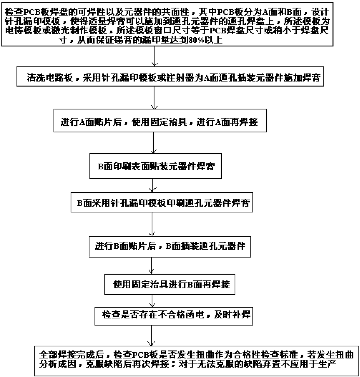
[0033] The application background of this embodiment is to weld the printed circuit board of epoxy resin glass fiber cloth copper-clad laminate, the thickness is 1.6, and because the tin-lead self-flow soldering process is used, it is required that the inserted components can withstand soldering for more than 1 minute at a high temperature of 235 degrees Celsius process. According to attached figure 1 The circuit board welding method in the embodiment comprises the steps:

[0034] (1) Check the solderability of the PCB pad and the coplanarity of the components. The PCB board is divided into A side and B side, and the pinhole missing printing template is designed so that an appropriate amount of solder paste can be applied to the through-hole components. On the through-hole pad, the template is an electroformed template or a laser-made template, and the size of the template window is equal to or slightly smaller than the size of the PCB pad, so as to ensure that the amount of ...


PUM

PropertyMeasurementUnit
Thicknessaaaaaaaaaa
Thicknessaaaaaaaaaa

Abstract

The invention provides a method for welding a circuit board. The method comprises the following steps: (1) checking weldability of a PCB welding disc, and coplanarity of an element, wherein a PCB comprises a plane A and a plane B and is designed as a pinhole skip printing template; (2) cleaning the circuit board, and applying a welding paste to elements inserted into through holes in the plane A by using the pinhole skip printing template or an injector; (3) performing plane A pasting, and welding the plane A by using a fixing jig; (4) pasting an element welding paste to a printing surface ofthe plane B; (5) printing the plane B with a hole element welding paste by using the pinhole skip printing template; (6) performing plane B pasting, and inserting through hole elements into the planeB; (7) welding the plane B by using the fixing jig; (8) checking whether unqualified welding points are resulted or not, and performing welding replenishing in time; (9) after welding is completed, checking whether the PCB has distortion or not as a qualification inspection standard, analyzing reasons of distortion, overcoming defects, performing welding again, and discarding products which defects which cannot be overcome.

Description

technical field [0001] The invention relates to the field of welding testing, in particular to a welding method for PCB boards. Background technique [0002] Printed circuit board (PCB) is the support of circuit components and devices in electronic products. The quality of PCB welding has a great impact on electronic products. With the rapid development of electronic technology, the density of PCB is getting higher and higher, and there are more and more layers, and there are mixed circuit boards containing surface mount components and through-hole components at the same time. More and more complex, there are several methods in the prior art: [0003] (1) Manual welding: use manual operation, use electric soldering iron or other heating tools to melt the welding wire to realize the connection between component pins and PCB board pads, manual welding has less investment, quick product changeover, mature technology, and requirements for welding personnel Low, flexible weldin...

Claims


Application Information

Patent Timeline
IPC IPC(8): H05K3/34
CPCH05K3/34H05K2203/04H05K2203/163
Inventor 李军曾凡国陈明侨
Owner 汉通(沧州)电子有限公司
Why Eureka
Try Eureka