
Organic electroluminescent device

An electroluminescence device and luminescence technology, which are applied in the fields of organic light-emitting devices, organic light-emitting device parameters, organic semiconductor devices, etc., and can solve the problems that the power efficiency of organic electroluminescent devices needs to be improved.

Active Publication Date: 2018-07-31
NOVALED GMBH
View PDF34 Cites 2 Cited by
  • Summary
  • Abstract
  • Description
  • Claims
  • Application Information

AI Technical Summary

Problems solved by technology

[0007] However, the power efficiency of organic electroluminescent devices still needs to be improved

Method used


Image

  • Organic electroluminescent device
  • Organic electroluminescent device
  • Organic electroluminescent device

Examples


Embodiment

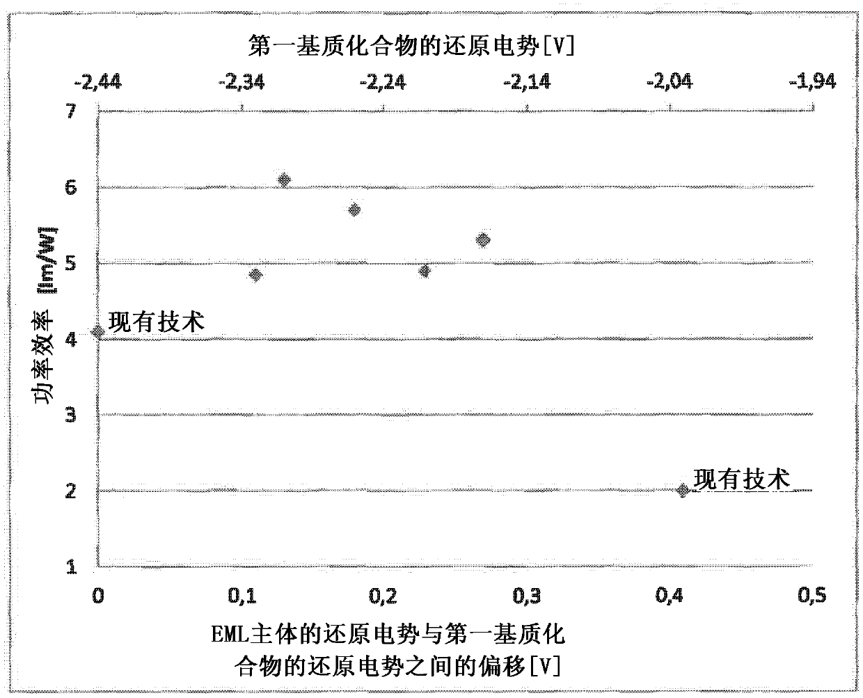
[0347] Various dipole moments and reduction potentials of representative examples of the first host compound were measured below. The results are given in Table 4 below.

[0348] Table 4: Dipole moments and reduction potentials of representative examples of first host compounds

[0349]

[0350]

[0351]

[0352] Various dipole moments for representative examples of second host compounds are calculated below. The results are given in Table 5 below.

[0353] Table 5: Dipole moments of representative examples of second host compounds

[0354]

[0355] *) The two conformers have a total energy difference of 1 kJ / mol. Therefore, two conformers exist at room temperature.

[0356] synthesis program

[0357] Synthesis of Compound ETM-3 ([1,1':4',1"-terphenyl]-3-ylbis(2-methylnaphthalen-1-yl)borane)

[0358]

[0359] 1. Tetrakis(3-bromophenyl)stannane stage 1

[0360] Sn(m-C 6 h 4 Br) 4 : 1,3-Dibromobenzene (5.89 g, 24.97 mmol) was dissolved in 60 mL of e...


PUM


Abstract

The present invention relates to an organic electroluminescent device comprising an anode, a cathode, an emission layer, an undoped electron transport layer comprising a first matrix compound, and anelectron injection layer comprising a second matrix compound and an. alkali organic complex and / or alkali halide, wherein the undoped electron transport layer and the electron injection layer are arranged between the emission layer and the cathode, wherein the reduction potential of the first matrix compound is less negative than, the reduction potential of 9,10-di(naphthalen-2-yl)anthracene and more negative than the reduction potential of 4,4'- bis(4,6-diphenyl- 1,3,5-triazin-2-yl)biphenyl, wherein the reduction potential in both cases is measured against Fc / Fc+ in tetrahydrofurane; and thedipole moment of the first matrix compound is selected >= 0 Debye and <= 2.5 Debye and the dipole moment of the second matrix compound is selected > 2.5 and < 10 Debye.

Description

technical field [0001] The present invention relates to organic electroluminescent devices. Background technique [0002] Organic Light Emitting Diodes (OLEDs) are self-emitting devices that feature wide viewing angles, excellent contrast, fast response, high brightness, excellent driving voltage characteristics, and color reproduction. A typical OLED includes an anode, a hole transport layer (HTL), an emission layer (EML), an electron transport layer (ETL), and a cathode stacked in sequence on a substrate. In this regard, HTLs, EMLs and ETLs are thin films formed of organic and / or organometallic compounds. [0003] When a voltage is applied to the anode and the cathode, holes injected from the anode move to the EML through the HTL, and electrons injected from the cathode move to the EML through the ETL. The holes and electrons recombine in the EML to generate excitons. When the excitons drop from the excited state to the ground state, light is emitted. The injection and...

Claims


Application Information

Patent Timeline
Patent Type & Authority Applications(China)
IPC IPC(8): H01L51/52
CPCH10K85/654H10K85/322H10K85/6572H10K50/11H10K2101/40H10K50/16H10K50/171H10K2101/50H10K85/658H10K85/615H10K85/623H10K85/657H10K2101/00
Inventor 多玛果伊·帕维奇科卡斯滕·洛特维金塔斯·扬库什雷吉娜·卢舍蒂尼特兹杰罗姆·加尼耶
Owner NOVALED GMBH
Learn More