Post processing method of silk screen printed silver nanowire transparent conductive thin film

A technology of transparent conductive film and silver nanowire, applied in the direction of nanotechnology, nanotechnology, conductive layer on insulating carrier, etc., can solve the problems of low surface roughness mechanical flexibility, high processing cost, poor flexibility, etc., and achieve low Effects of surface roughness, improvement of mechanical flexibility, and improvement of electrical conductivity

Inactive Publication Date: 2018-08-03
NANJING UNIV OF POSTS & TELECOMM
View PDF4 Cites 4 Cited by
  • Summary
  • Abstract
  • Description
  • Claims
  • Application Information

AI Technical Summary

Problems solved by technology

[0005] Technical problem to be solved: In order to overcome the deficiencies in the prior art, this application proposes a post-processing method for screen-printed silver nanowire transparent conductive film. The silver nanowire transparent conductive film prepared by this method has higher conductivity It can be used as a flexible transparent electrode in various optoelectronic devices, and can solve technical problems such as high processing cost, high resistivity and poor flexibility in the prior art.

Method used


Image

  • Post processing method of silk screen printed silver nanowire transparent conductive thin film

Examples


Embodiment 1

[0020] Step 1: Place the silver nanowire ink on the mask of the screen printing instrument at 40 mm s -1 Printing speed, 30N printing pressure, the squeegee passes through the mask plate at a constant speed, and the silver nanowire pattern is printed on the PET substrate;

[0021] The second step: heat and anneal the silver nanowire pattern at 120 °C for 5 min to evaporate the solvent, then perform plasma treatment for 10 min, and the plasma power is 180 W, and then rinse the silver nanowire pattern with deionized water;

[0022] Step 3: The silver nanowire pattern rinsed with deionized water is then heated and annealed at 120 °C for 15 minutes, and then rinsed with deionized water to remove residual additives;

[0023] Step 4: Heat and anneal the silver nanowire pattern from which the residual additives have been removed at 120° C. for 15 min to prepare a silver nanowire transparent conductive film.

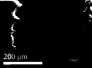
[0024] The SEM spectrum of the silver nanowire transparent conductive film...

Embodiment 2

[0026] Step 1: Place the silver nanowire ink on the mask of the screen printing instrument at 40 mm s -1 Printing speed, 30N printing pressure, the squeegee passes through the mask plate at a constant speed, and the silver nanowire pattern is printed on the PET substrate;

[0027] The second step: the silver nanowire pattern was heated and annealed at 120 °C for 5 min to evaporate the solvent, followed by plasma treatment for 10 min with a plasma power of 190 W, and then the silver nanowire pattern was rinsed with deionized water;

[0028] Step 3: The silver nanowire pattern rinsed with deionized water is then heated and annealed at 120 °C for 15 minutes, and then rinsed with deionized water to remove residual additives;

[0029] Step 4: Heat and anneal the silver nanowire pattern from which the residual additives have been removed at 120° C. for 15 min to prepare a silver nanowire transparent conductive film.

Embodiment 3

[0031] Step 1: Place the silver nanowire ink on the mask of the screen printing instrument at 40 mm s -1 Printing speed, 30N printing pressure, the squeegee passes through the mask plate at a constant speed, and the silver nanowire pattern is printed on the PET substrate;

[0032] The second step: the silver nanowire pattern was heated and annealed at 120 °C for 5 minutes to evaporate the solvent, followed by plasma treatment for 15 minutes with a plasma power of 180 W, and then the silver nanowire pattern was rinsed with deionized water;

[0033] Step 3: The silver nanowire pattern rinsed with deionized water is then heated and annealed at 120 °C for 15 minutes, and then rinsed with deionized water to remove residual additives;

[0034] Step 4: Heat and anneal the silver nanowire pattern from which the residual additives have been removed at 120° C. for 15 min to prepare a silver nanowire transparent conductive film.


PUM

PropertyMeasurementUnit
transmittivityaaaaaaaaaa

Abstract

The invention discloses a post processing method of a silk screen printed silver nanowire transparent conductive thin film. By performing annealing, cleaning and plasma processing on a silk screen printed silver nanowire pattern, contact resistance between the silver nanowires can be lowered, and remarkable increasing of the thin film electrical conductivity is realized; by virtue of the post processing process, the bonding strength between the silver nanowires, and between the silver nanowires and a substrate also can be improved, thereby improving the mechanical flexibility of the thin filmand enabling the transparent conductive thin film to maintain relatively high photoelectric stability in a mechanical deformation condition; and the silver nanowire transparent conductive thin film prepared by the method is relatively high in electrical conductivity and light transmittance, relatively low in surface roughness and excellent in mechanical flexibility, and can be used as a flexible transparent electrode to be applied to various photoelectric devices.

Description

technical field [0001] The invention belongs to the technical field of printed electronics, and in particular relates to a post-processing method of screen-printed silver nanowire transparent conductive film. Background technique [0002] In recent years, flexible / wearable devices, such as smart watches, bracelets, optoelectronic displays, energy storage, medical electronics, etc., have received more and more attention. Among them, as one of the basic components, transparent conductive films play a vital role in the performance of various optoelectronic devices. Indium tin oxide (ITO) is a transparent conductive film widely used at present. However, higher processing costs and limited indium reserves have kept the price of ITO high. Therefore, the development of new low-cost transparent conductive films is one of the most important frontier topics at present. [0003] Silver nanowire transparent conductive films are regarded as the most promising next-generation transpa...

Claims


Application Information

Patent Timeline
Patent Type & Authority Applications(China)
IPC IPC(8): H01B5/14H01B1/02H01B13/00B82Y30/00
CPCH01B5/14B82Y30/00H01B1/02H01B13/00
Inventor 李东东赖文勇黄维
Owner NANJING UNIV OF POSTS & TELECOMM
Why Eureka
Try Eureka