Antenna structure for terahertz microbolometer and preparation method thereof

A microbolometer and antenna structure technology, applied in the field of terahertz detection and imaging, can solve the problems of high absorption rate in difficult wide frequency bands, low absorption rate of metal films, etc. Effective absorption area effect

Active Publication Date: 2020-12-11
UNIV OF ELECTRONICS SCI & TECH OF CHINA
View PDF8 Cites 0 Cited by
  • Summary
  • Abstract
  • Description
  • Claims
  • Application Information

AI Technical Summary

Problems solved by technology

[0006] The purpose of the present invention is: to solve the problem that the metal thin film in the common microbridge structure in the existing terahertz microbolometer has low absorption rate, and the antenna absorption structure has frequency selectivity, and it is difficult to obtain high absorption rate in a wide frequency band Problem, the present invention provides an antenna structure for a terahertz microbolometer and its preparation method

Method used


Image

  • Antenna structure for terahertz microbolometer and preparation method thereof
  • Antenna structure for terahertz microbolometer and preparation method thereof
  • Antenna structure for terahertz microbolometer and preparation method thereof

Examples


preparation example Construction

[0044] In order to solve the problem that the metal thin film in the common microbridge structure in the existing terahertz microbolometer has a low absorption rate, but the antenna absorption structure has frequency selectivity, and it is difficult to obtain a high absorption rate in a wide frequency band, the present invention provides a An antenna structure for a terahertz microbolometer and a preparation method thereof.

[0045] An antenna structure for a terahertz microbolometer, the antenna structure 40 is a planar antenna structure located in a multilayer film on the bridge deck of a terahertz microbolometer microbridge structure 10, and the antenna structure 40 has a thickness of 5-40nm metal thin film. The antenna structure 40 of the present invention integrates a layer of planar antenna in the multilayer film of the terahertz microbolometer microbridge structure bridge deck. The antenna structure has a large metal film area and is used as a metal film absorption laye...

Embodiment 1

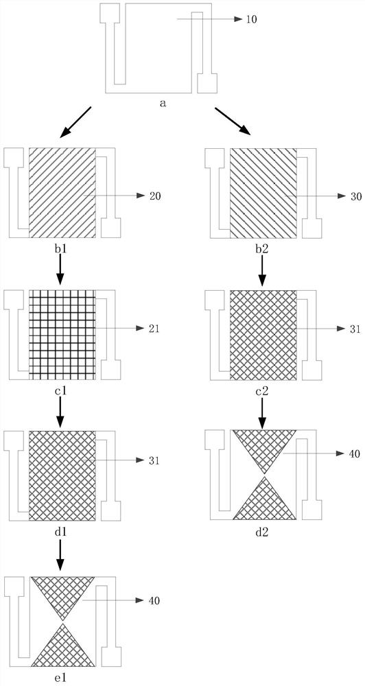
[0059] A RIE modified antenna structure for terahertz microbolometers, the preparation process is as follows figure 1 shown.

[0060] Terahertz microbolometer microbridge structure such as figure 1 Shown in a. Clean the surface of the micro-bridge structure, remove the contamination of the interface of the sensitive layer of the bridge deck and the interface of the substrate circuit, and bake the substrate at 200°C to remove the moisture on the surface.

[0061] The silicon nitride dielectric film was prepared by PECVD growth technology, the PECVD deposition temperature was 250°C, and the SiH 4 with NH 3 The flow ratio is 30 / 150, and the thickness of the prepared silicon nitride film is 200nm, such as figure 1 Shown in b1.

[0062] The silicon nitride film is etched through the first reactive ion etching process to form a surface microstructure. Etching gas is CHF 3 and O 2 . set CHF 3 with O 2 The flow ratio is 20:5, the RF power is 400W, the reaction chamber pres...


PUM

PropertyMeasurementUnit
thicknessaaaaaaaaaa
thicknessaaaaaaaaaa
thicknessaaaaaaaaaa

Abstract

The invention provides an antenna structure for a terahertz microbolometer and a preparation method thereof, and the technical field of terahertz detection and imaging. A planar antenna is integrated in the thin film, which is also used as the metal film absorption layer. The broadband absorption of the metal film and the coupling of the antenna to specific frequencies are used to enhance the absorption to achieve broadband and high absorption of terahertz waves. The invention adopts the RIE process to modify and treat the dielectric substrate layer or the antenna layer under the antenna to form a surface microstructure, increase the effective absorption area of ​​the antenna and the metal thin film absorption layer, and improve the absorption efficiency.

Description

technical field [0001] The invention relates to the technical field of terahertz detection and imaging, in particular to an antenna structure for a terahertz microbolometer and a preparation method thereof. Background technique [0002] Terahertz (THz) waves refer to electromagnetic radiation with a frequency ranging from 0.1 to 10 THz (wavelength 3 mm to 30 μm), and its electromagnetic spectrum lies between the microwave and infrared bands. Therefore, terahertz systems take advantage of both electronics and optics. For a long time, due to the lack of effective terahertz radiation generation and detection methods, people's understanding of the properties of electromagnetic radiation in this band is very limited, so that this band is called the terahertz gap in the electromagnetic spectrum. This band is also the last frequency window in the electromagnetic spectrum to be fully studied. Compared with electromagnetic waves in other bands, terahertz electromagnetic waves have ...

Claims


Application Information

Patent Timeline
Patent Type & Authority Patents(China)
IPC IPC(8): H01Q17/00
CPCH01Q17/00H01Q17/008
Inventor 苟君牛青辰王军黎威志蒋亚东
Owner UNIV OF ELECTRONICS SCI & TECH OF CHINA
Why Eureka
Try Eureka