Novel gallium-oxide(Ga2O3)-based-PIN structure-included ultraviolet photoelectric detector and preparation method thereof

A technology of electrical detectors and gallium oxide, which is applied in circuits, electrical components, semiconductor devices, etc., can solve the problems of insensitivity of ultraviolet detectors, achieve high lateral carrier mobility, strong stability, improve responsivity and The effect of stability

Inactive Publication Date: 2018-08-07
无锡华亿外延科技有限公司 +1
View PDF4 Cites 14 Cited by
  • Summary
  • Abstract
  • Description
  • Claims
  • Application Information

AI Technical Summary

Problems solved by technology

The multi-period non-doped superlattice used as the structure of the absorbing layer can effectively solve the problem of insensitivity of the ultraviolet detector due to the similar ionization coefficients of electrons and holes in the ultraviolet photodetector, which helps to improve Detector Responsivity and Stability to UV Signal

Method used


Image

  • Novel gallium-oxide(Ga2O3)-based-PIN structure-included ultraviolet photoelectric detector and preparation method thereof

Examples


Embodiment 1

[0029] The present invention will be further described below in conjunction with the accompanying drawings.

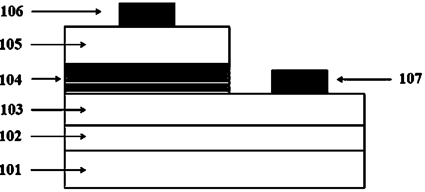
[0030] like figure 1 Shown is a novel gallium oxide-based PIN structure ultraviolet photodetector, including a substrate (101), a buffer layer (102), an n-type Ga 2 o 3 Layer (103), non-doped i-type NiO / TiO 2 Superlattice absorption layer (104), p-type Ga 2 o 3 layer (105), in n-type Ga 2 o 3 The n-type ohmic electrode (107) drawn on the layer (103), on the p-type Ga 2 o 3 The p-type ohmic electrode (106) drawn on the layer (105).

[0031] The substrate (101) is a sapphire crystal.

[0032] The buffer layer (102) is Ga 2 o 3 layer with a thickness of 900 nm.

[0033] The n-type Ga 2 o 3The layer (103) has a thickness of 700nm and is doped with Si, wherein the doping concentration of Si is greater than 6×10 19 cm -3 .

[0034] The non-doped i-type NiO / TiO 2 Superlattice absorbing layer (104), the NiO layer thickness in a single period is 5nm, TiO 2 Th...

Embodiment 2

[0041] like figure 1 Shown is a novel gallium oxide-based PIN structure ultraviolet photodetector, including a substrate (101), a buffer layer (102), an n-type Ga 2 o 3 Layer (103), non-doped i-type NiO / TiO 2 Superlattice absorption layer (104), p-type Ga 2 o 3 layer (105), in n-type Ga 2 o 3 The n-type ohmic electrode (107) drawn on the layer (103), on the p-type Ga 2 o 3 The p-type ohmic electrode (106) drawn on the layer (105).

[0042] The substrate (101) is silicon crystal.

[0043] The buffer layer (102) is Ga 2 o 3 layer with a thickness of 100 nm.

[0044] The n-type Ga 2 o 3 The layer (103) has a thickness of 1000nm and is doped with Si, wherein the doping concentration of Si is greater than 8×10 19 cm -3 .

[0045] The non-doped i-type NiO / TiO 2 Superlattice absorbing layer (104), the NiO layer thickness in a single period is 10nm, TiO 2 The layer thickness was 10 nm.

[0046] The non-doped i-type NiO / TiO 2 The number of repetition periods of the ...

Embodiment 3

[0052] like figure 1 Shown is a novel gallium oxide-based PIN structure ultraviolet photodetector, including a substrate (101), a buffer layer (102), an n-type Ga 2 o 3 Layer (103), non-doped i-type NiO / TiO 2 Superlattice absorption layer (104), p-type Ga 2 o 3 layer (105), in n-type Ga 2 o 3 The n-type ohmic electrode (107) drawn on the layer (103), on the p-type Ga 2 o 3 The p-type ohmic electrode (106) drawn on the layer (105).

[0053] The substrate (101) is silicon crystal.

[0054] The buffer layer (102) is Ga 2 o 3 layer with a thickness of 1000 nm.

[0055] The n-type Ga 2 o 3 The layer (103) has a thickness of 2000nm and is doped with Si, wherein the doping concentration of Si is greater than 8×10 19 cm -3 .

[0056] The non-doped i-type NiO / TiO 2 Superlattice absorbing layer (104), the NiO layer thickness in a single period is 3nm, TiO 2 The layer thickness was 8 nm.

[0057] The non-doped i-type NiO / TiO 2 The number of repeating periods of the su...


PUM


Abstract

The invention discloses a novel gallium-oxide(Ga2O3)-based-PIN structure-included ultraviolet photoelectric detector and a preparation method thereof. The ultraviolet photoelectric detector is composed of a substrate (101), a buffer layer (102), an n type Ga2O3 layer (103), and an non-doped i type NiO / TiO2 superlattice absorber layer (104), a p type Ga2O3 layer (105), an n type ohmic electrode (107) led out at the n type Ga2O3 layer (103), and a p type ohmic electrode (106) led out at the p type Ga2O3 layer (105) that are arranged successively from bottom to top. According to the invention, with the multi-period non-doped i type NiO / TiO2 superlattice as the absorption layer, a problem that the ultraviolet detector is insensitive because of the similar ionization coefficients of the electron and hole in the ultraviolet photoelectric detector is solved; and the responsivity and stability of the detector to the UV signal are improved. The ultraviolet photoelectric detector having advantages of novel structure and high sensitivity is suitable for deep ultraviolet detection.

Description

technical field [0001] The invention relates to the field of semiconductor optoelectronic devices, in particular to a novel gallium oxide-based PIN structure ultraviolet photodetector and a preparation method thereof. Background technique [0002] Ultraviolet photodetectors have important application value and development prospects in both military and civilian applications, such as: ultraviolet warning and guidance, detection of hydrocarbon combustion flames, detection of biochemical genes, research in ultraviolet astronomy, short-distance communication and skin disease treatment, etc. Commercial ultraviolet detectors are mainly made of silicon, which need to filter out the incident visible light and infrared light and need to be equipped with cooling components. In contrast, wide-gap semiconductors such as SiC, diamond, GaN, and Ga 2 o 3 etc., naturally avoid these problems of silicon detectors; where Ga 2 o 3 The band gap at room temperature is about 4.9eV, which is ...

Claims


Application Information

Patent Timeline
Patent Type & Authority Applications(China)
IPC IPC(8): H01L31/0352H01L31/105H01L31/18
CPCH01L31/035236H01L31/105H01L31/18Y02P70/50
Inventor 孙月静
Owner 无锡华亿外延科技有限公司
Why Eureka
Try Eureka