A kind of gan-based SBD frequency conversion circuit and its manufacturing method

A frequency conversion circuit and circuit technology, applied in the direction of circuits, electrical components, electric solid devices, etc., can solve problems such as large stress, device reliability, high power application limitations, and heat cannot be quickly exported, so as to avoid inhibition and avoid current The effect of pooling side benefits and avoiding current congestion

Active Publication Date: 2020-05-26
INST OF ELECTRONICS ENG CHINA ACAD OF ENG PHYSICS
View PDF5 Cites 0 Cited by
  • Summary
  • Abstract
  • Description
  • Claims
  • Application Information

AI Technical Summary

Problems solved by technology

Compared with GaAs, the research on (GaN)-based Schottky diode (SBD) terahertz devices and frequency conversion circuits is still in its infancy, especially the direction of on-chip integrated GaN-based SBD terahertz frequency conversion circuits. Due to the special hexagonal crystal system of GaN materials Due to structural and anti-corrosion characteristics, it is difficult to realize a GaAs-like substrate-free membrane (membrance) on-chip integration process through a selective wet etching process
However, in the GaAs-based SBD terahertz on-chip integrated frequency conversion circuit, due to the existence of the bonding glue, the large amount of heat generated in the Schottky junction and the LO oscillator cannot be quickly dissipated, resulting in the reliability and reliability of the device. High-power applications are limited. At the same time, due to the large stress in epitaxial GaN, it is difficult to thin gallium nitride (GaN) materials to less than 30 microns without cracking through thinning and polishing processes.
Therefore, there is no clear technical solution for on-chip integration of GaN-based SBD terahertz frequency conversion circuits.

Method used


Image

  • A kind of gan-based SBD frequency conversion circuit and its manufacturing method
  • A kind of gan-based SBD frequency conversion circuit and its manufacturing method
  • A kind of gan-based SBD frequency conversion circuit and its manufacturing method

Examples


Embodiment 1

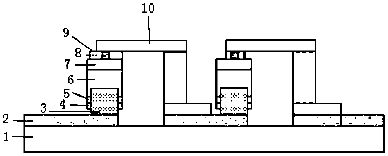
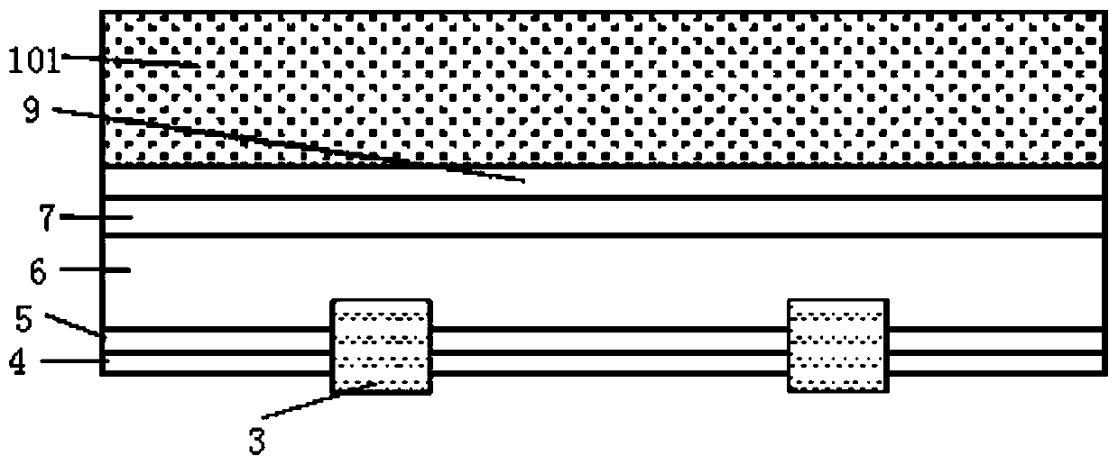
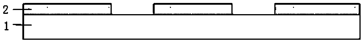
[0034] Such as figure 1As shown, this embodiment provides a GaN-based SBD frequency conversion circuit, including a substrate-based circuit and a vertical electrode-based GaN-based SBD device. The substrate-based circuit includes a substrate 1 and a first layer of metal 2 in sequence, The GaN-based SBD device based on vertical electrodes includes a second layer of metal 3, a first layer of dielectric layer 4, a GaN buffer layer 5, an n+GaN layer 6, an n-GaN layer 7, and a third layer of metal 8 from bottom to top. , the second layer of dielectric layer 9 and the fourth layer of metal 10, between the first layer of metal 2 and the second layer of metal 3 and / or between the first layer of metal 2 and the fourth layer of metal 10 through metal- The metals are directly bonded so that the connection points between the first layer metal and the second layer metal and / or the first layer metal and the fourth layer metal have the function of loading DC and AC signals. The metal-metal ...

Embodiment 2

[0056] Such as Figure 6 As shown, the symbols of the components in the second embodiment correspond to the symbols of the components in the embodiment. For example, the number of the substrate in the embodiment is 1, the number of the substrate in the second embodiment is 11, the number of the first metal layer in the first embodiment is 2, the number of the first metal layer in the second embodiment is 12, and so on. The material of each layer of the second embodiment is the same as that of the first embodiment, and the main difference between the second embodiment and the first embodiment lies in step (4). The step (4) of embodiment two is specifically as follows:

[0057] On the n-GaN layer 17, the second dielectric layer 19 is selectively deposited (it can be deposited using dielectric deposition equipment), and the n-GaN is removed by one or both of the photolithography process and the etching process. -GaN layer 17, exposing the n+GaN layer 16, and then using one or b...


PUM

PropertyMeasurementUnit
thicknessaaaaaaaaaa
thicknessaaaaaaaaaa
thicknessaaaaaaaaaa

Abstract

The invention discloses a GaN based SBD frequency conversion circuit, and belongs to the fields of preparation of Terahertz high-frequency devices and integrated circuits. The frequency conversion circuit comprises a circuit based on a diamond substrate and a GaN-based SBD device based on a vertical electrode, and the circuit based on the diamond substrate comprises the substrate, a first metal layer, a second metal layer, a first dielectric layer, a GaN buffer layer, an n+GaN layer, an n-GaN layer, a third metal layer, a second dielectric layer and a fourth metal layer from bottom to top successively. The invention also discloses a manufacturing method of the GaN based SBD frequency conversion circuit. Advantages of third-generation of wide gap semiconductor GaN and a diamond material areutilized fully and integrated, and the high-performance frequency conversion circuit with high power and high temperature reliability is realized.

Description

technical field [0001] The invention belongs to the field of preparation of terahertz high-frequency devices and integrated circuits, and in particular relates to a GaN-based SBD frequency conversion circuit and a manufacturing method thereof. Background technique [0002] Terahertz (THz) waves refer to electromagnetic waves with a frequency in the range of 0.1THz to 10THz, between microwaves and infrared rays, and have extremely important academic value and practical significance. In the direction of monolithic integrated terahertz frequency doubling and mixing circuits, GaAs-based SBD terahertz devices and on-chip integrated frequency conversion circuits have been developed for many years, and there are mature and clear technical routes, such as Master technology and substrate-free membrane (membrance) technology . Compared with GaAs, the research on (GaN)-based Schottky diode (SBD) terahertz devices and frequency conversion circuits is still in its infancy, especially th...

Claims


Application Information

Patent Timeline
Patent Type & Authority Patents(China)
IPC IPC(8): H01L21/18H01L25/00H01L25/16
CPCH01L21/187H01L25/16H01L25/50
Inventor 曾建平安宁李倩谭为
Owner INST OF ELECTRONICS ENG CHINA ACAD OF ENG PHYSICS
Why Eureka
Try Eureka