Preparation method of micro-nano die profiled groove

A mold and micro-nano technology, which is applied in the field of micro-nano mold groove preparation, can solve the problems of not meeting the performance requirements, jagged edges, large roughness, etc., and achieve strong wear resistance, small thermal expansion coefficient, and thermal conductivity. The effect of high coefficient

Inactive Publication Date: 2018-08-24
HENAN UNIV OF SCI & TECH
View PDF11 Cites 0 Cited by
  • Summary
  • Abstract
  • Description
  • Claims
  • Application Information

AI Technical Summary

Problems solved by technology

[0004] The purpose of the present invention is to provide a method for preparing micro-nano mold-shaped grooves, which overcomes the defects of jagged edges, large roughness and failure to meet performance requirements produced by laser etching by using vapor deposition and plasma etching processes

Method used


Image

  • Preparation method of micro-nano die profiled groove
  • Preparation method of micro-nano die profiled groove
  • Preparation method of micro-nano die profiled groove

Examples


preparation example Construction

[0030] A method for preparing a micro-nano mold groove, comprising the following steps:

[0031] Step 1. Coating: In a plasma-enhanced chemical vapor deposition coating machine, a Si sheet is used as a base material, and a SiC film is deposited on the surface of the base material;

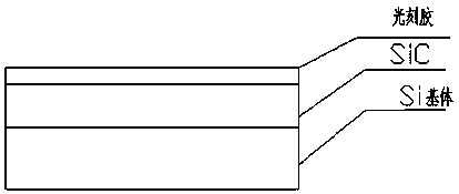
[0032] Step 2, photolithography: transfer the pattern of the mask to the SiC film layer by photolithography;

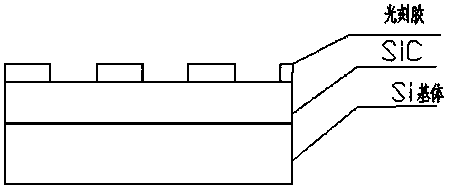
[0033] Step 3, etching: using an inductively coupled plasma etching machine to etch grooves on the SiC film layer.

[0034] The photolithography process of the present invention adopts a photoresist mask; the etching process adopts an ICP plasma etching process.

[0035] The present invention is realized in the following ways: Figure 1 to Figure 4 The steps of the fabrication process are illustrated.

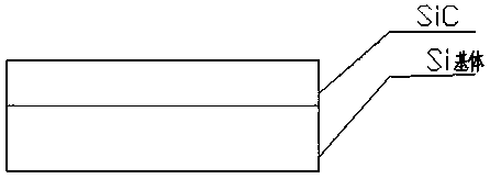
[0036] Step 1, PECVD coating:

[0037] Such as figure 1 As shown, on the PECVD chemical vapor deposition coating machine, the SiC film layer is deposited on the surface of the Si subst...

Embodiment 1

[0053] A method for preparing a micro-nano mold groove, comprising the following steps:

[0054] (1) Coating: Deposit SiC thin film on the surface of Si base material on PECVD chemical vapor deposition coating machine;

[0055] (2) Photolithography: transfer the pattern of the mask to the SiC film layer by photolithography;

[0056] (3) Etching: use an etching machine to etch grooves on the SiC film layer.

[0057] In step (1), a 5 μm SiC thin film is deposited by PECVD chemical vapor phase method. SiH 4 、CH 4 The gas flow ratio is 6:1, the power setting is 300w, and the air pressure is 1Pa.

[0058] In step (3), an ICP etching machine is used to etch grooves on the SiC film layer. Etching gas using CF 4 , SF 6 , O 2 For etching gas, the flow rate ratio is 7:1:1, and the total flow rate is 40 sccm. The power of the upper / lower electrodes is set to 550 / 300W, and the air pressure is set to 1Pa.

[0059] The etched groove is "凵" type.

Embodiment 2

[0061] A method for preparing a micro-nano mold groove, comprising the following steps:

[0062] (1) Coating: Deposit SiC thin film on the surface of Si base material on PECVD chemical vapor deposition coating machine;

[0063] (2) Photolithography: transfer the pattern of the mask to the SiC film layer by photolithography;

[0064] (3) Etching: use an etching machine to etch grooves on the SiC film layer.

[0065] In step (1), a SiC film of 8 μm was deposited by PECVD chemical vapor phase method. SiH 4 、CH 4 The gas flow ratio is 2:1, the power setting is 300w, and the air pressure is 1Pa.

[0066] In step (3), an ICP etching machine is used to etch grooves on the SiC film layer. Etching gas using CF 4 , SF 6 , O 2 Etching gas, the flow rate ratio is 6:1:1, and the total flow rate is 30 sccm. The power of the upper / lower electrodes is set to 580 / 350W, and the air pressure is set to 3Pa.

[0067] The etched groove is "U" shape.


PUM

PropertyMeasurementUnit
thicknessaaaaaaaaaa
Mohs hardnessaaaaaaaaaa

Abstract

The invention discloses a preparation method of a preparation method of a micro-nano die profiled groove. The preparation method comprises a coating step: taking a Si wafer as a base material in a plasms-enhanced chemical vapor deposition coating machine; depositing a SiC film on the surface of the base material; a photoetching step: transferring a pattern of a mask to the SiC film by using the photoetching process; and an etching step: etching a profiled groove on the SiC film by adopting an inductive coupled plasma etching machine. The die profiled groove prepared by the method disclosed bythe invention is high in heat conductivity coefficient, small in heat expansion coefficient, strong in fire resistance and wear resistance, and has anti-corrosion effect on the potassium hydroxide alkali solution and the hydrogen fluoride acid solution and like corrosives.

Description

technical field [0001] The present invention designs the technical field of mold preparation, and specifically designs a method for preparing micro-nano mold grooves. Background technique [0002] With the development of mold devices in the direction of micro-nano, the commonly used mold steel is far from meeting the requirements. At the sub-micron scale, conventional processing techniques can no longer meet this performance requirement. For laser etching processing, 10 μm basically reaches its processing limit. However, the principle of laser is hot-melt processing, the edge is jagged, and the roughness is very large, which cannot meet the mold groove processing technology of this size. Some ceramic materials such as Al 2 o 3 、SiN x , has extremely strong corrosion resistance, and cannot be processed by wet corrosion methods. [0003] In the micro-nano size, the material performance requirements for making such mold-shaped grooves are very high, requiring high strengt...

Claims


Application Information

Patent Timeline
Patent Type & Authority Applications(China)
IPC IPC(8): B81C1/00
CPCB81C1/00349B81C1/00531B81C2201/0132B81C2201/0156B81C2201/018
Inventor 闫焉服杨文玲王广欣高志廷傅山泓吴丹凤
Owner HENAN UNIV OF SCI & TECH
Why Eureka
Try Eureka